Solidtron, N-mos vcs, thinpak – Silicon Power SMCT TA 32N14_N-MOS VCS, ThinPak User Manual
Page 5

Application Notes
A1. Junction Temperature Calculation
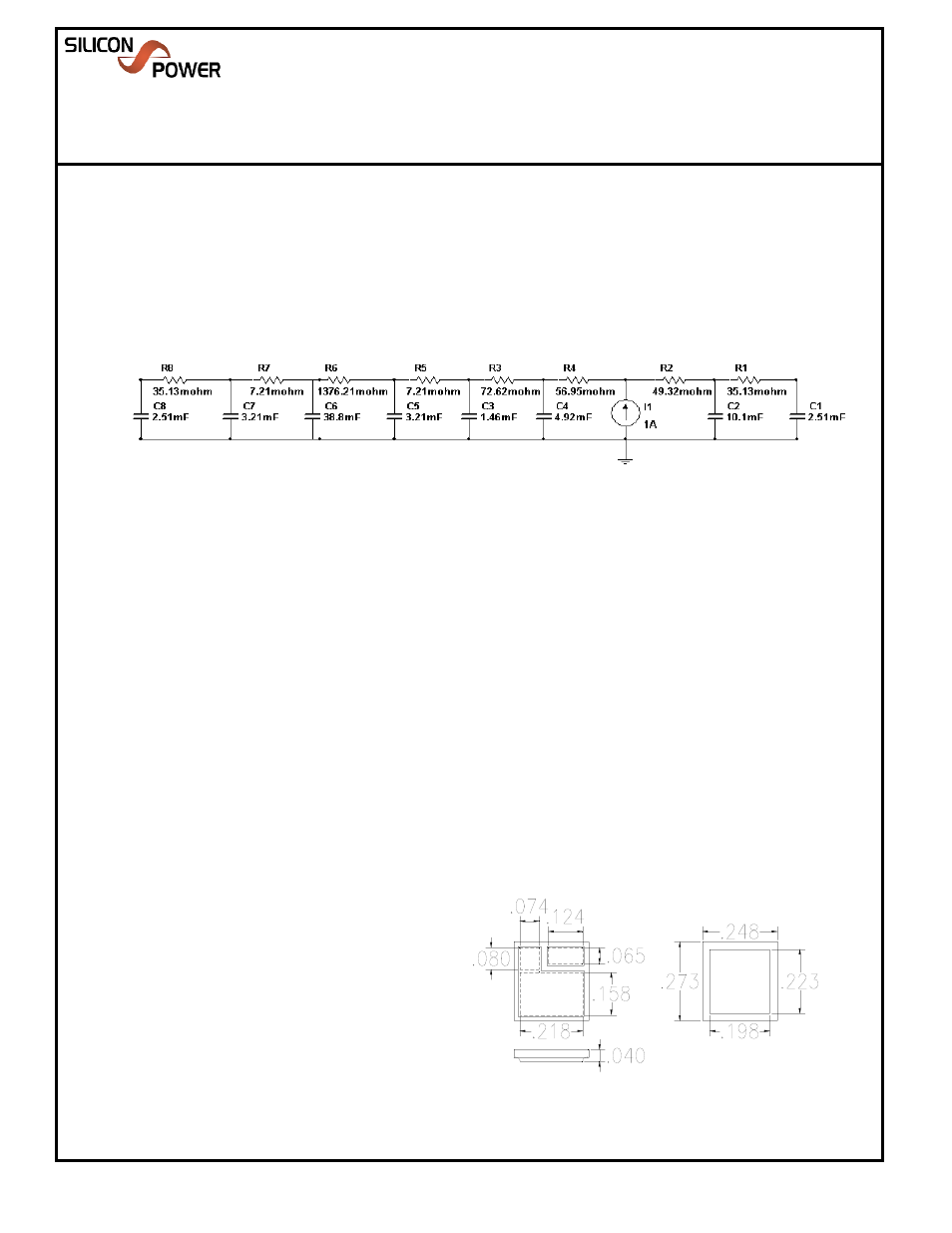
The figure below shows a lump model of the thermal properties of the size 4 thinPak packaged VCS, from the 2-mil solder on
the top of the lid on the left to the 2-mil solder on the bottom of the device on the right. By adding the user's lump model of the
rest of the thermal system the user can calculate the junction and case temperature rise under any operating condition.
A2. Calculation of Pulses to Failure for Intermediate/Long Pulse Widths
The user may calculate the Number of Pulses to failure (N
F
) for long to intermedeiate pulse widths (not covered in the typical
performance curve section) by applying the junction temperature rise (dT), calculated as described in A1, to the formula
N
F
=(300/dT)9 .
Anode
(Bottom) Side
Interface
Cathode-Gate
(Top) Side
Interface
Device
Junction
SMCTTA32N14A10
Solidtron
TM
N-MOS VCS, ThinPak
TM
Data Sheet (Rev 2 - 07/10/2008)
275 Great Valley Parkway
Malvern, PA 19355
Ph: 610-407-4700
www.siliconpower.com
Packaging and Handling
CAO 05/28/09
A3. Use of Gate Return Bond Area.
The MCT was designed for high di/dt applications. An independent cathode connection or "Gate Return Bond Area" was
provided to minimize the effects of rapidly changing Anode-Cathode current on the Gate control voltage, (V=L*di/dt). It is
therefore, critcal that the user utilize the Gate Return Bond Area as the point at which the gate driver reference (return) is
attached to the VCS device.
Top
Cathode-Gate
Bottom
Anode
Side
1. All metal surfaces are tinned using 63pb/37sn solder.
2. Installation reflow temperature should not exceed
260
o
C or internal package degradation may result.
3. Package may be cooled from either top or bottom
(See Figure 7)
4. As with all MOS gated devices, proper handling
procedures must be observed to prevent electrostatic
discharge which may result in permanent damage to
the gate of the device
Package Dimensions
CAO 05/28/09
