10 d/a channel 0 output, 11 d/a channel 1 output – Advantech PCI-1710 User Manual
Page 46

42
PCI-1710/1710HG User's Manual
4.10 D/A Output Channel 0 BASE+10
and BASE+11
The write-only registers of BASE+10 and BASE+11 accept data for
D/A Channel 0 output.
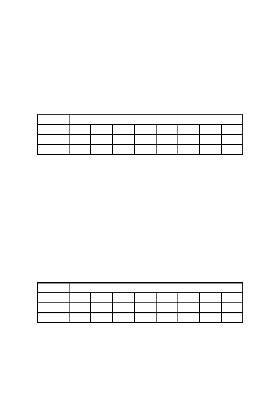
Table 4-10: Registers for D/A channel 0 data
DA11 ~ DA0 Digital to Analog data
DA0 is the LSB and DA11 is the MSB of the D/A data.
4.11 D/A Output Channel 1 BASE+12
and BASE+13
The write-only registers of BASE+12 and BASE+13 accept data for
the D/A channel 1 output.
Table 5-11: Registers for D/A channel 1 data
DA11 ~ DA0 Digital to Analog data
DA0 is the LSB and DA11 is the MSB of the D/A data.
Write
D/A Output Channel
Bit #
7
6
5
4
3
2
1
0
BASE+11
DA11
DA10
DA9
DA8
BASE+10
DA7
DA6
DA5
DA4
DA3
DA2
DA1
DA0
Write
D/A Output Channel
Bit #
7
6
5
4
3
2
1
0
BASE+13
DA11
DA10
DA9
DA8
BASE+12
DA7
DA6
DA5
DA4
DA3
DA2
DA1
DA0
