Ar c hive inf o rma ti o n archive informa tion – Communication Concepts EB63 Engineering Bulletin User Manual
Page 2
AR
C
HIVE INF
O
RMA
TI
O
N
ARCHIVE INFORMA
TION
EB63
2
RF Application Reports
The bias diode D2 has been mounted in the heatsink for
temperature tracking. The cathode is pressed into the
heatsink and the anode extends through the circuit board.
(See Figure 9.) Both input and output transformers are 4:1
turns ratio (16:1 impedance ratio) to achieve low input SWR
across the specified band and a high saturation capability.
T1* is made from FairRite Products, ferrite beads, material
#77, .375
″ O.D. x .187/.200″ I.D. x .44L″. T2* is made from
Stackpole Co. ferrite sleeves #57-3238-7D.
When using this design, it is important to interconnect the
ground plane on the bottom of the board to the top; especially
at the emitters of the MRF454s. Eyelets were used in this
design, which are easier to apply, but #18 AWG wire can
be used. On the photomask, (see Figure 10) “:” signifies
where the ground plane has been interconnected. The letter
“O” designates where the 4 – 40 screws are installed to
fasten the board to the heatsink. 6 – 32 nuts are used as
spacers on the 4 – 40 screws between the board and the
heatsink to keep the board from touching the heatsink.
THE DESIGN
This amplifier was designed for simplicity. The design goal
was to allow repeatability of assembly and reduce the
number of components used. The amplifier will accept Single
Side Band or Amplitude Modulation without external
switching. A carrier operated relay circuit is on the same
layout to make this an easy amplifier to add on to any suitable
radio with an RF output of 1.0 – 5.0 Watts. All components
used are readily available at most distributors and are
relatively inexpensive.
P out,
POWER OUTPUT
, W
ATTS (PEP)
200
180
160
140
120
100
80
60
40
20
0
0
1
2
3
4
5
P
in
, POWER INPUT, (WATTS PEP)
Figure 1. P
out
vs. P
in
, 30 MHz, 13.6 Vdc
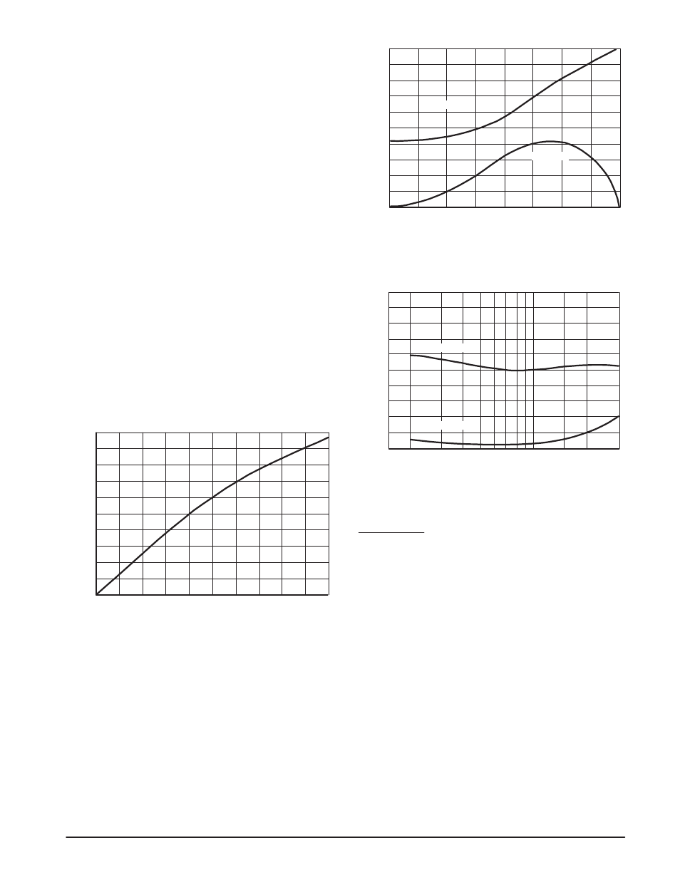
IMD, INTERMODULA
TION DIST
OR
TION, (dB)
200
180
160
140
120
100
80
60
40
-50
-45
-40
-35
-30
-25
P
out
, POWER OUTPUT, (WATTS PEP)
3rd Order
5th Order
Figure 2. Intermodulation Distortion Versus
P
out
, 30 MHz, 13.6 Vdc
IMD DIST
OR
TION (dB)
3
2
-40
1.5
-30
-20
5
7
10
15
20
30
FREQUENCY (MHz)
3rd Order
5th Order
Figure 3. IMD vs. Frequency,
P
out
= 140 Watt PEP, 13.6 Vdc
* Ref: Application Notes
1. AN749 BroadBand Transformers and Power Combining Tech-
niques for RF – H. Granberg
2. AN762 Linear Amplifiers for Mobile Operation – H. Granberg
NOTE: Parts and Kits for this amplifier are available from:
Communication Concepts, Inc. (CCI)
508 Millstone Drive
Beavercreek, Ohio 45434-5840
(513) 426-8600