Pam8407 new product, Pin descriptions, Functional block diagram – Diodes PAM8407 User Manual
Page 2: Absolute maximum ratings, Pam8407
PAM8407
Document number: DS36815 Rev. 1 - 2
2 of 12
www.diodes.com
January 2014
© Diodes Incorporated
PAM8407
New Product
A PRODUCT LINE OF
DIODES INCORPORATED
2x3W Stereo Differential Input Class D Audio Amplifier
with Up/Down Volume Control
Pin Descriptions
PIN Number
PIN Name
Description
1
RINP
Positive Input of Right Channel Power Amplifier.
2
RINN
Negative Input of Right Channel Power Amplifier.
3
SD
Full Chip Shutdown Control Input (active low).
4 UP
Volume UP Control (active low)
Ground Connection.
5
DOWN
Volume down Control (active low)
6,12,13 GND
Ground.
7
LINN
Negative Input of Left Channel Power Amplifier.
8
LINP
Positive Input of Left Channel Power Amplifier.
9,16 VDD
Power
Supply.
10
LOUTP
Positive Output of Left Channel Power Amplifier.
11
LOUTN
Negative Output of Left Channel Power Amplifier.
14
ROUTN
Negative Output of Right Channel Power Amplifier.
15
ROUTP
Positive Output of Right Channel Power Amplifier.
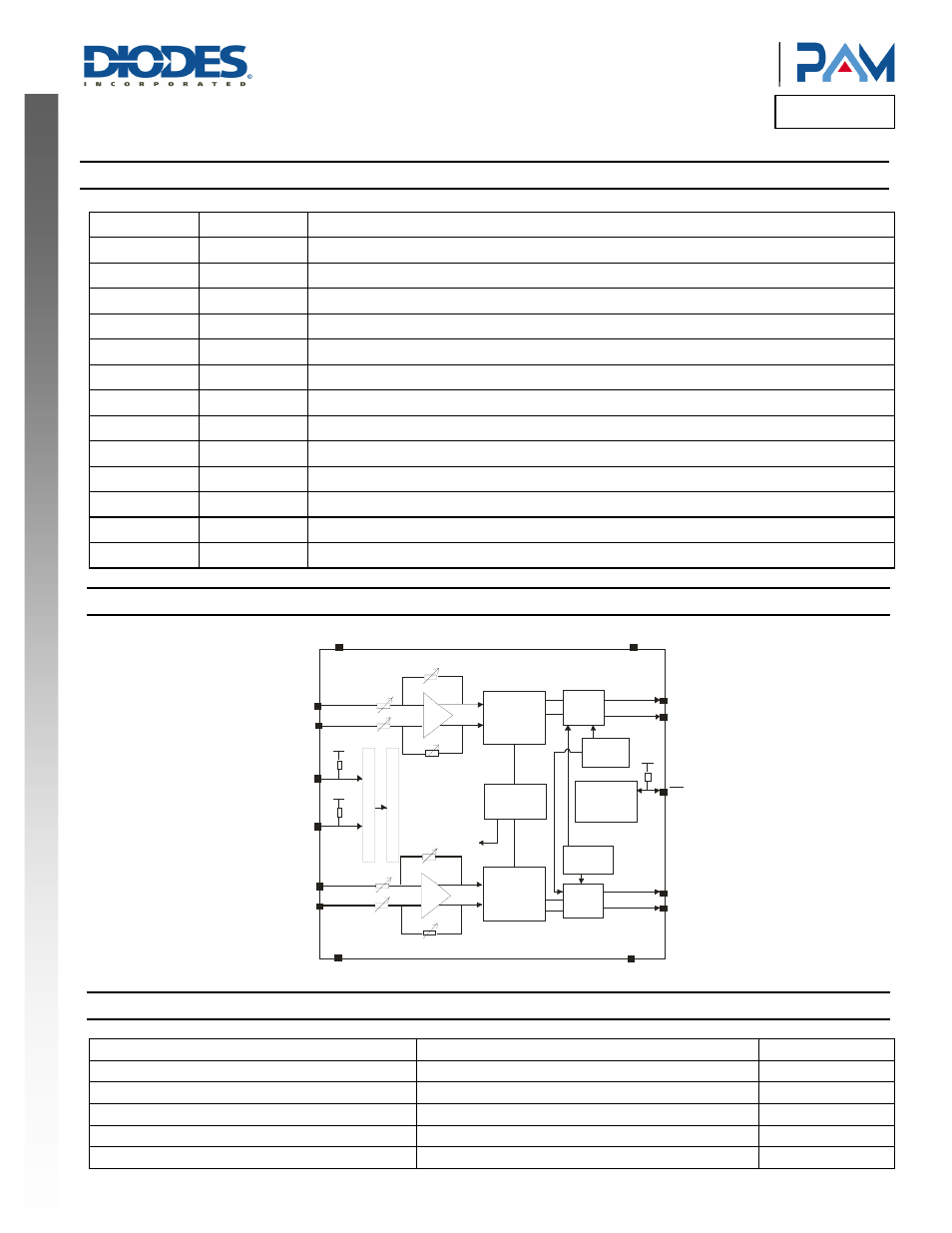
Functional Block Diagram
In
te
rf
a
c
e C
o
n
tr
o
l
A
tt
enuat
io
n
D
e
c
o
d
e
r
V D D
R IN P
LIN N
VDD
GND
LOU T P
LOU T N
R OU T N
R OU T P
GN D
MODULATOR
DRIVER
INTERNAL
OSCILLATOR
O S C
BIAS
AND
REFERENCES
MODULATOR
D R IVER
Thermal
Protection
Current
Protection
DOWN
SD
VD D
+
-
R IN N
UP
+
-
LIN P
VD D
VD D
Absolute Maximum Ratings
(@T
A
= +25°C, unless otherwise specified.)
Parameter Rating
Unit
Supply Voltage (VDD)
6.5
V
Pins Input Voltage (SD, UP, Down, IN)
-0.3 to VDD+0.3
V
Storage Temperature
-65 to +150
°C
Maximum Junction Temperature
+150
°C
Junction to ambient thermal resistance
40
°C/W