Diodes PAM8407 User Manual
Pam8407 new product, Features, Pin assignments
PAM8407
Document number: DS36815 Rev. 1 - 2
1 of 12
www.diodes.com
January 2014
© Diodes Incorporated
PAM8407
New Product
A PRODUCT LINE OF
DIODES INCORPORATED
2x3W Stereo Differential Input Class D Audio Amplifier
with Up/Down Volume Control
Description
The PAM8407 is a filter-less Class-D amplifier with high SNR and
differential input that helps eliminate noise. Advanced 32-step
Up/Down volume control minimizes external components and allows
speaker volume control.
The PAM8407 supports 2.5V to 6V operation make it idea for up to 4
cells alkaline battery applications.
Features like greater than 87% efficiency and small PCB area make
the PAM8407 Class-D amplifier ideal for portable applications. The
output uses a filter-less architecture minimizing the number of
external components and PCB area whilst providing a high
performance, simple and lower cost system.
The PAM8407 built in auto recovery SCP (short circuit protection) and
thermal shutdown.
The PAM8407 is available in SO-16 package.
Features
3W Output at 10% THD with a 4Ω load and 5V Supply
2.4W Output at 1% THD with a 4Ω Load and 5V Supply
2.5V to 6.0V VDD Operating
Fully
Differential
Input
Filterless, Low Quiescent Current and Low EMI
Low
THD+N
32-stepUp/Down Volume Control from -80dB to 24dB
Superior Low Noise: 60uV
Minimize Pop/Clip Noise
Auto Recovery Short Circuit Protection
Thermal
Shutdown
Pb-Free
SO-16
Package
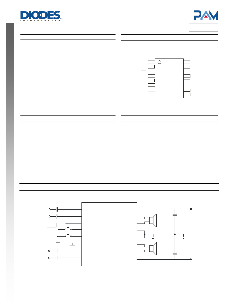
Pin Assignments
SO-16
LOUTP
LOUTN
UP
VDD
ROUTP
VDD
ROUTN
GND
15
9
10
11
12
13
14
16
GND
RINN
GND
DOWN
LINN
SD
1
2
3
4
5
6
7
8
P
A
M
84
07
XX
XY
W
W
L
L
RINP
LINP
Applications
PC
Speaker
Wireless
Speaker
Home Sound Systems
Active
Speakers
Docking
stations
Typical Applications Circuit
6 GND
GND 13
5 DOWN
7 LINN
VDD 16
8 LINP
GND 12
1 RINP
ROUTN 14
2 RINN
ROUTP 15
LOUTP 10
VDD 9
4 UP
3 SD
LOUTN 11
PAM8407
0 1
.
uF
C6
V
DD
4Ω
1uF
C2
RINN
0 1
. uF
C8
LINP
SHDN
ON
0 1
.
uF
C5
RINP
0 1
.
uF
C7
LINN
4Ω
V
DD
1uF
C2