Pam8124 new prod uc t, Absolute maximum ratings, Recommended operating conditions – Diodes PAM8124 User Manual
Page 3: Electrical characteristics
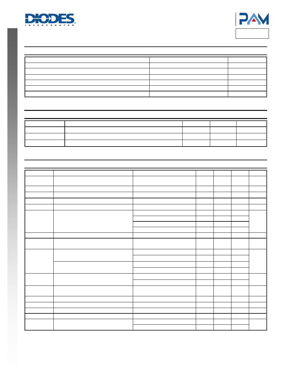
PAM8124
Document number: DS36627 Rev. 1 - 2
3 of 15
October 2013
© Diodes Incorporated
PAM8124
NEW PROD
UC
T
A Product Line of
Diodes Incorporated
Absolute Maximum Ratings
(@T
A
= +25°C, unless otherwise specified.)
Parameter Rating
Unit
Supply Voltage (VCC)
28 V
Logic Input Voltage (SDN, MUTE, GAIN0, GAIN1, SE_BTL)
-0.3 to V
CC
+0.3
V
Analog Input Voltage (LIN, RIN)
-0.3 to +5.5
V
Storage Temperature
-65 to +150
°C
Maximum Junction Temperature
150
°C
Junction to ambient thermal resistance
40
°C/W
Recommended Operating Conditions
(@T
A
= +25°C, unless otherwise specified.)
Symbol Parameter
Min
Max
Unit
V
CC
Supply Voltage
10
26
V
T
A
Operating Ambient Temperature Range
-40 +85 °C
T
J
Junction Temperature Range
-40 +125 °C
Electrical Characteristics
(@T
A
= +25°C, V
CC
= 24V, Gain = 20dB, R
L
= 8Ω unless otherwise specified.)
Symbol Parameter
Test
Conditions
Min
Typ
Max
Units
|VOS|
Class-D output offset voltage(measured
differently)
V
i
= 0V, A
V
= 36dB
20
100
mV
I
CC(q)
Quiescent supply current
SDN = 2.5V, MUTE = 0V, No Load
25
40
mA
I
CC(MUTE)
Quiescent supply current in mute mode
MUTE = 2.5V, No load
25
40
mA
I
CC(SDN)
Quiescent current in shutdown mode
SDN = 0.8V, No load
30
60
µA
R
DS(ON)
Drain-source on-state resistance
I
O
= 0.5A
150 mΩ
G Gain
GAIN1 = 0.8V, GAIN0 = 0.8V
18
20
22
dB
GAIN1 = 0.8V, GAIN0 = 2.5V
24
26
28
GAIN1 = 2.5V, GAIN0 = 0.8V
30
32
34
GAIN1 = 2.5V, GAIN0 = 2.5V
34
36
38
Mute Attenuation
Vi = 1Vrms
-60
dB
PSRR
Power Supply Rejection Ratio
V
RIPPLE
= 200mVpp,
f = 1kHz,gain = 20dB
-52 dB
P
O
Output Power at 1% THD+N
R
L
= 4Ω, f = 1kHz
14
W
R
L
= 8Ω, f = 1kHz
8
Output Power at 10% THD+N
R
L
= 4Ω, f = 1kHz
18
R
L
= 8Ω, f = 1kHz
10
THD+N
Total harmonic distortion + noise
R
L
=4Ω, f = 1kHz, Po = 10W
0.15
%
R
L
= 8Ω, f = 1kHz, Po = 5W
0.08
Vn
Output integrated noise floor
20Hz to 22kHz, A-weighted,
Gain = 20dB
200
µV
Cs Crosstalk
P
O
= 1W, f = 1kHz, Gain = 20dB
-70
dB
SNR Signal-to-noise
ratio
THD+N<1%,
f = 1kHz, Gain = 20dB
92
dB
OTP
Thermal trip point
160 °C
OTH Thermal
hysteresis
60 °C
fosc Oscillator
frequency
SE_BTL = 2.5V
250
300
350
kHz
SE_BTL = 0.8V
360