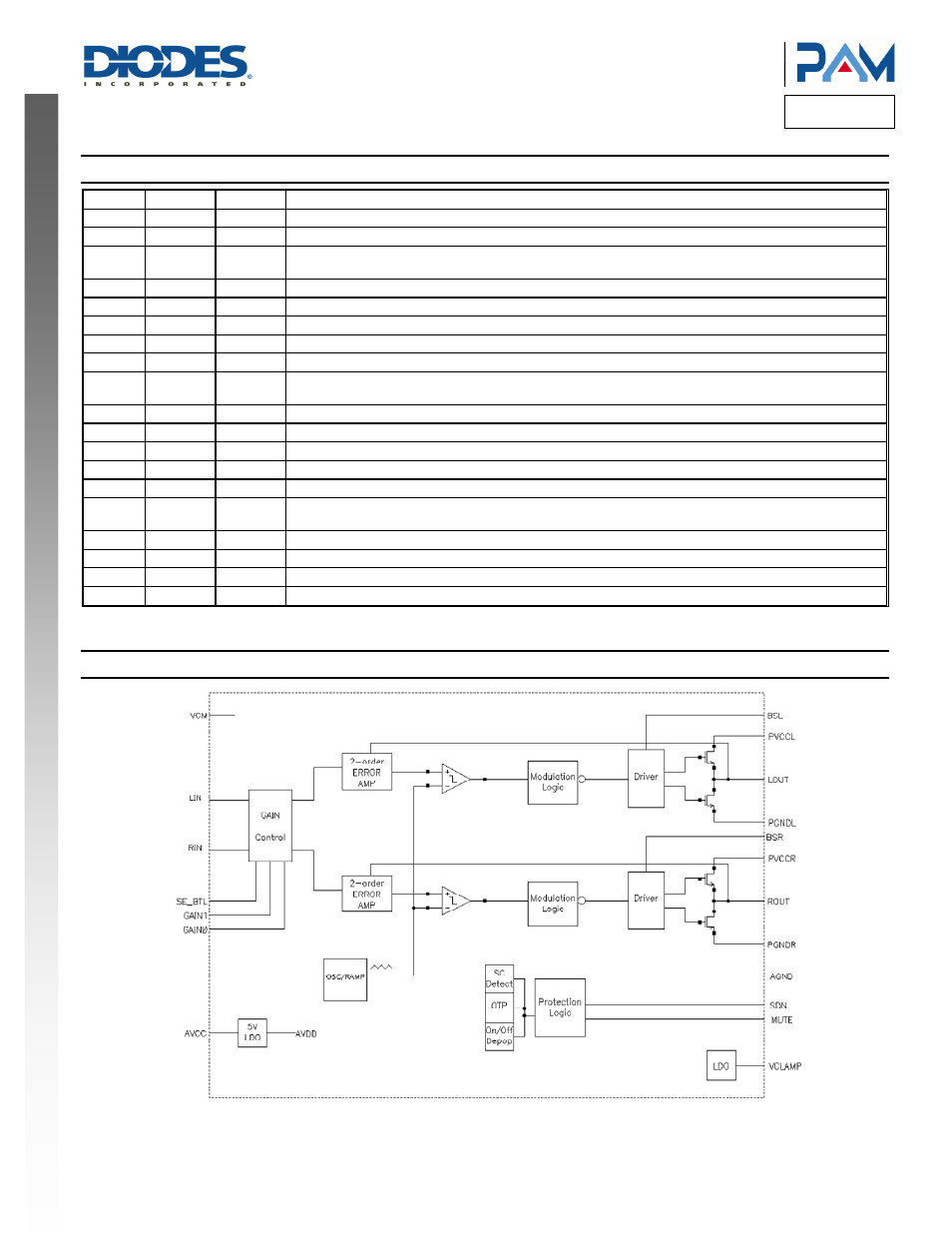
Pam8124 new prod uc t, Pin descriptions, Functional block diagram – Diodes PAM8124 User Manual
Page 2
PAM8124
Document number: DS36627 Rev. 1 - 2
2 of 15
October 2013
© Diodes Incorporated
PAM8124
NEW PROD
UC
T
A Product Line of
Diodes Incorporated
Pin Descriptions
Pin Name I/O/P
Function
1, 3
PVCCL
P
Power supply for left channel H-bridge, not connected to PVCCR or AVCC
2
SDN
I
Shutdown signal for IC (low = shutdown, high = operational). TTL logic levels with compliance to AVCC
4 MUTE I
A logic high on this pin disables the outputs. A low on this pin enables the outputs. TTL logic levels with
compliance to AVCC
5
LIN
I
Audio input for left channel
6
RIN
I
Audio input for right channel
7
VCM
O
Reference for analog cells
8, 9
AGND
P
Analog ground for digital/analog cells in core
10, 12
PVCCR
P
Power supply for right channel H-bridge, not connected to PVCCL or AVCC
11 VCLAMP P
Internally generated voltage supply for bootstrap. Not to be used as a supply or connected to any
component other than the decoupling capacitor.
13, 14
PGNDR
P
Power ground for right channel H-bridge
15
ROUT
O
Class-D H-bridge output for right channel
16
BSR
I/O
Bootstrap I /O for right channel H-bridge
17
GAIN1
I
Gain select most-significant bit. TTL logic levels with compliance to AVCC
18
GAIN0
I
Gain select least-significant bit. TTL logic levels with compliance to AVCC
19 SE_BTL I
A logic low on this pin enables one single-ended input in BTL configuration. A logic high on this pin
enables two inputs in SE/BTL configuration. TTL logic levels with compliance to AVCC
20
AVCC
P
High-voltage analog power supply
21
BSL
I/O
Bootstrap I /O for left channel H-bridge
22
LOUT
O
Class-D H-bridge output for left channel
23, 24
PGNDL
P
Power ground for left channel H-bridge
Functional Block Diagram