Diodes LMV321/ 324/ 358 User Manual
Page 3
LMV321/ 358/ 324
Document number: DS33196 Rev. 7 - 2
3 of 15
January 2013
© Diodes Incorporated
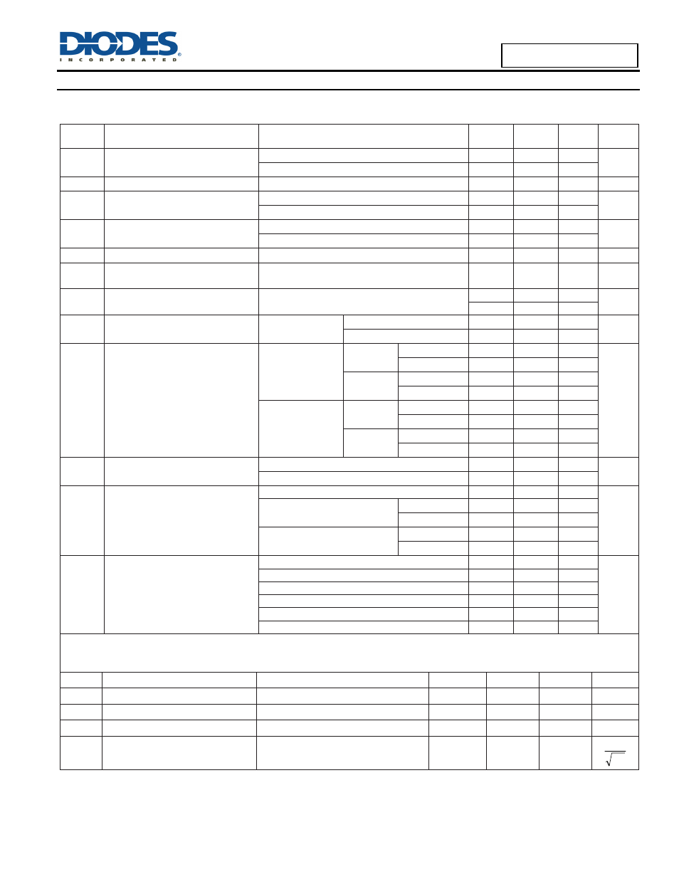
LMV321/ 324/ 358
Electrical Characteristics
(cont.) (@T
A
= +25°C, unless otherwise specified.)
5V DC Electrical Characteristics
Unless otherwise specified, all limits guaranteed
for T
A
= +25°C, V
+
= 5V, V
-
= 0V, V
CM
= 2.0V, V
O
= V
+
/2 and R
L
> 1 MΩ.
Symbol
Parameter Test
Conditions
Min
(Note 8)
Typ
(Note 7)
Max
(Note 8)
Unit
V
OS
Input Offset Voltage
T
A
= +25°C
1.7
7
mV
T
A
= full range
9
TCV
OS
Input Offset Voltage Average Drift
5
µV/°C
I
B
Input Bias Current
T
A
= +25°C
15
250
nA
T
A
= full range
500
I
OS
Input Offset Current
T
A
= +25°C
5
50
nA
T
A
= full range
150
CMRR Common Mode Rejection Ratio
0V
≤ V
CM
≤ 4.0V
50 65 dB
PSRR Power Supply Rejection Ratio
2.7V
≤ V
+
≤ 5V
V
O
= 1V, V
CM
= 1V
50 60 dB
V
CMR
Input Common-Mode Voltage Range For CMRR
≥ 50dB
0 -0.2
V
4.2
4.0
A
V
Large Signal Voltage Gain
R
L
= 2 kΩ (Note 9)
T
A
= +25°C
15 100
V/mV
T
A
= full range
10
V
O
Output Swing
R
L
= 2 kΩ to 2.5V
High level
T
A
= +25°C
V
+
- 300
V
+
-50
mV
T
A
= full range
V
+
- 400
Low level
T
A
= +25°C
50
300
T
A
= full range
400
R
L
= 10 kΩ to 2.5V
High level
T
A
= +25°C
V
+
- 100
V
+
-10
T
A
= full range
V
+
- 200
Low level
T
A
= +25°C
10
180
T
A
= full range
280
I
O
Output Short Circuit Current
Sourcing, V
O
= 0V
5 60
mA
Sinking, V
O
= 5V
10 90
I
S
Supply Current
LMV321 Single amplifier
110
140
µA
LMV358 Both amplifiers
T
A
= +25°C
190
340
T
A
= full range
600
LMV324 All four amplifiers
T
A
= +25°C
340
680
T
A
= full range
1100
θ
JA
Thermal Resistance Junction-to-
Ambient
SOT353 (Note 10)
330
°C/W
SOT25 (Note 10)
250
TSSOP-14 (Note 10)
100
MSOP-8 (Note 10)
203
SO-8 (Note 10)
150
SO-14 (Note 10)
83
5V AC Electrical Characteristics
Unless otherwise specified, all limits guaranteed for T
A
= 25°C, V
+
= 5V, V
-
= 0V, V
CM
= 2.0V, VO = V
+
/2 and R
L
> 1 MΩ.
Boldface limits apply at the temperature extremes.
SR
Slew Rate
(Note 11)
1
V/µs
GBWP Gain-Bandwidth
Product
C
L
= 200pF
1
MHz
Φ
m
Phase Margin
60
Deg
G
m
Gain Margin
10
dB
e
n
Input-Referred Voltage Noise
f > 50 kHz
23
Z
H
nV
Notes:
7. Typical values represent the most likely parametric norm as determined at the time of characterization. Actual typical values may vary over time
and will also depend on the application and configuration. The typical values are not tested and are not guaranteed on shipped production material.
8. All limits are guaranteed by testing or statistical analysis.
9. R
L
is connected to V-. The output voltage is 0.5V
≤ V
O
≤ 4.5V.
10. All numbers are typical, and apply for packages soldered directly onto a PC board in still air.
11. Connected as voltage follower with 3V step input. Number specified is the slower of the positive and negative slew rates.