Absolute maximum ratings, Recommended operating conditions, Electrical characteristics – Diodes LMV321/ 324/ 358 User Manual
Page 2
LMV321/ 358/ 324
Document number: DS33196 Rev. 7 - 2
2 of 15
January 2013
© Diodes Incorporated
LMV321/ 324/ 358
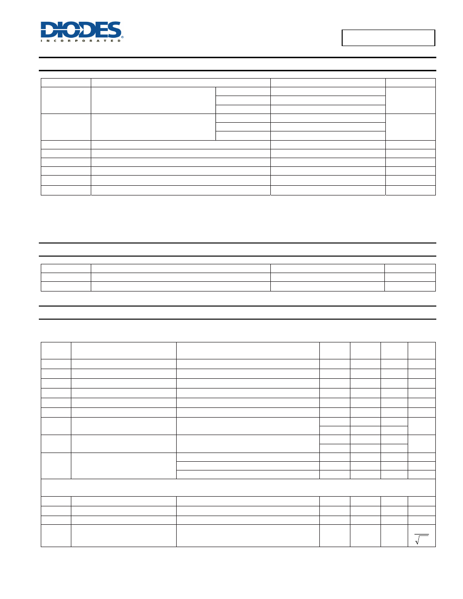
Absolute Maximum Ratings
(Note 4) (@T
A
= +25°C, unless otherwise specified.)
Symbol
Parameter
Rating
Unit
ESD HBM
Human Body Model ESD Protection
LMV321 4.0
KV
LMV358 4.0
LMV324 4.5
ESD MM
Machine Model ESD Protection
LMV321 350
V
LMV358 350
LMV324 250
Differential Input Voltage
±Supply Voltage
V
V
+
-V
-
Supply Voltage
5.5
V
Output Short Circuit to V
+
(Note 5)
Output Short Circuit to V
-
(Note
6)
T
ST
Storage Temperature
-65 to +150
°C
T
J
Maximum Junction Temperature
+150
°C
Notes:
4. Absolute Maximum Ratings indicate limits beyond which damage to the device may occur. Operating Ratings indicate conditions for which the
device is intended to be functional, but specific performance is not guaranteed. For guaranteed specifications and the test conditions, see the
Electrical Characteristics.
5. Shorting output to V+ will adversely affect reliability.
6. Shorting output to V- will adversely affect reliability.
Recommended Operating Conditions
(@T
A
= +25°C, unless otherwise specified.)
Symbol
Parameter
Rating
Unit
V
+
-V
-
Supply Voltage
2.7 to 5.5
V
T
A
Operating Ambient Temperature Range
-40 to +125
°C
Electrical Characteristics
(@T
A
= +25°C, unless otherwise specified.)
2.7V DC Electrical Characteristics
Unless otherwise specified, all limits guaranteed for T
A
= +25°C, V
+
= 2.7V, V
-
= 0V, V
CM
= 1.0V, V
O
= V
+
/2 and R
L
> 1 MΩ.
Symbol
Parameter Test
Conditions
Min
(Note 8)
Typ
(Note 7)
Max
(Note 8)
Unit
V
OS
Input Offset Voltage
1.7
7
mV
TCV
OS
Input Offset Voltage Average Drift
5
µV/°C
I
B
Input Bias Current
10
nA
I
OS
Input Offset Current
5
50
nA
CMRR Common Mode Rejection Ratio
0V
≤ V
CM
≤ 1.7V
50 63 dB
PSRR Power Supply Rejection Ratio
2.7V
≤ V
+
≤ 5V, V
O
= 1V
50 60 dB
V
CMR
Input Common-Mode Voltage Range For CMRR
≥ 50dB
0 -0.2
V
1.9
1.7
V
O
Output Swing
R
L
= 10 kΩ to 1.35V
V
+
- 100
V
+
- 20
mV
20
100
I
S
Supply Current
LMV321 Single amplifier
110
140
µA
LMV358 Both amplifiers
190
340
µA
LMV324 All four amplifiers
340
680
µA
2.7V AC Electrical Characteristics
Unless otherwise specified, all limits guaranteed for T
A
= +25°C, V
+
= 2.7V, V
-
= 0V, V
CM
= 1.0V, V
O
= V
+
/2 and R
L
> 1 MΩ.
GBWP Gain-Bandwidth
Product
C
L
= 200 pF
1
MHz
Φm
Phase Margin
60
Deg
Gm Gain
Margin
10
dB
e
n
Input-Referred Voltage Noise
f > 50 kHz
23
Z
H
nV