Typical application circuit, Application details – Diodes LMN200B01 User Manual
Page 8
DS30651 Rev. 7 - 2
8 of 10
LMN200B01
www.diodes.com
T
C
U
D
O
R
P
W
E
N
Vin
Control
D
E
S
B
G
C
Q1
PNP
Q2
NMOS
R2
470
R1
10K
R3
37K
LOAD
DDTB142JU
DSNM6047
Vout
5v Supply
Vout
Gnd
Vin
Control
U2
Voltage Regulator
IN
OUT
Control Logic
Circuit (PIC,
Comparator
etc)
U1
Vin
OUT1
GND
Diodes Inc.
U3
LNM200B01
1
3
2
4
5
6
E_Q1
D_Q2
G_Q2
S_Q2
B_Q1
C_Q1
Load Switch
Point of
Load
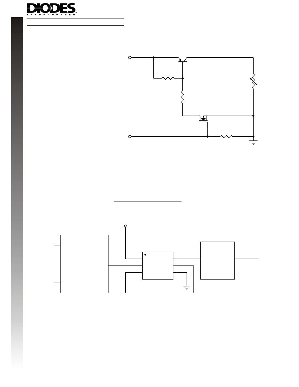
Typical Application Circuit
Fig. 19 Circuit Diagram
Fig. 20
•
PNP Transistor (DDTB142JU) and N-MOSFET
(DSNM6047) with gate pull-down resistor integrated
as one in LMN200B01 can be used as a discrete
entity for general purpose applications or as an
integrated circuit to function as a Load Switch. When
it is used as the latter as shown in Fig 19, various
input voltage sources can be used as long as it does
not exceed the maximum ratings of the device.
These devices are designed to deliver continuous
output load current up to a maximum of 200 mA. The
MOSFET Switch draws no current, hence loading of
control circuit is prevented. Care must be taken for
higher levels of dissipation while designing for higher
load conditions. These devices provide high power
and also consume less space. The product mainly
helps in optimizing power usage, thereby conserving
battery life in a controlled load system like portable
battery powered applications. (Please see Fig. 20
for one example of a typical application circuit used
in conjunction with voltage regulator as a part of a
power management system)
Application Details