Electrical characteristics, N-channel, P-channel – Diodes DMHC3025LSD User Manual
Page 3
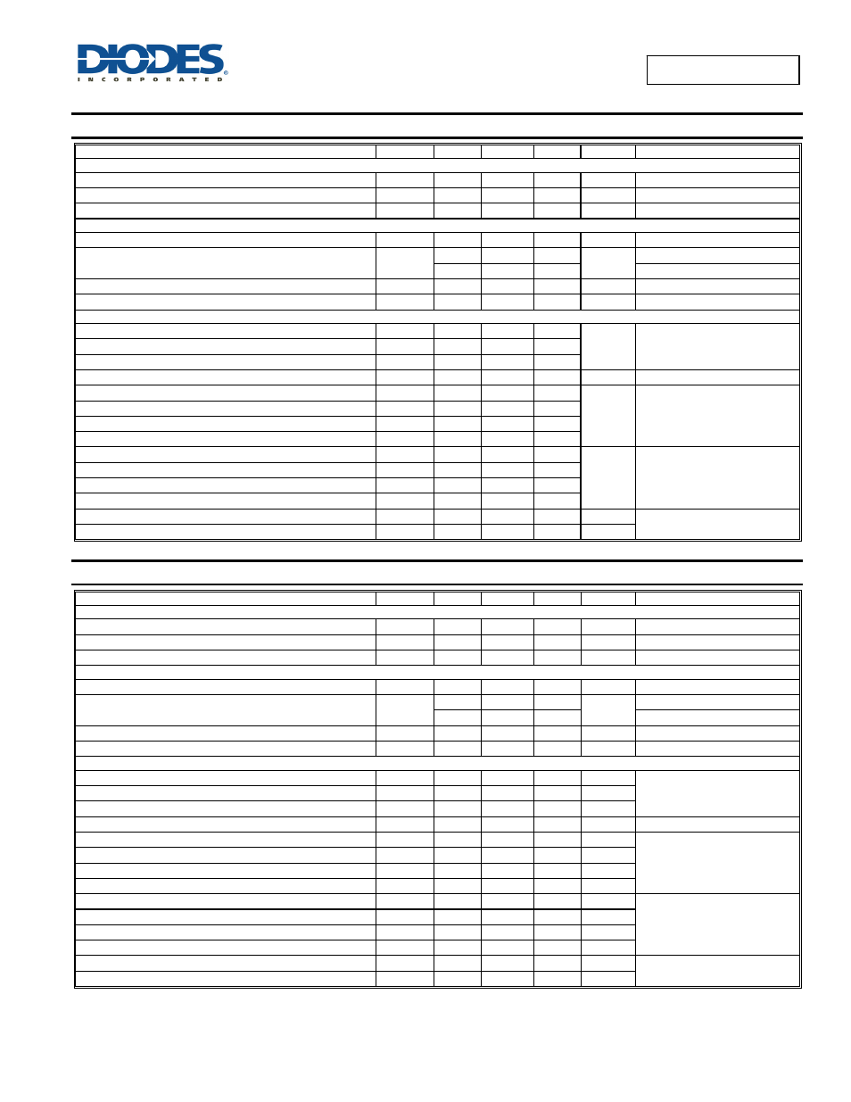
DMHC3025LSD
Document number: DS35821 Rev. 4 - 2
3 of 9
November 2013
© Diodes Incorporated
DMHC3025LSD
NEW PROD
UC
T
ADVAN
CE I
N
F
O
RM
ATI
O
N
Electrical Characteristics
N-CHANNEL
(@T
A
= +25°C, unless otherwise specified.)
Characteristic
Symbol
Min
Typ
Max
Unit
Test Condition
OFF CHARACTERISTICS (Note 6)
Drain-Source Breakdown Voltage
BV
DSS
30
—
— V
V
GS
= 0V, I
D
= 250μA
Zero Gate Voltage Drain Current
I
DSS
— — 0.5
μA
V
DS
= 30V, V
GS
= 0V
Gate-Source Leakage
I
GSS
— — ±1
μA
V
GS
= ±20V, V
DS
= 0V
ON CHARACTERISTICS (Note 6)
Gate Threshold Voltage
V
GS(th)
1 — 2 V
V
DS
= V
GS
, I
D
= 250μA
Static Drain-Source On-Resistance
R
DS (ON)
—
19 25
mΩ
V
GS
= 10V, I
D
= 5A
—
26 40
V
GS
= 4.5V, I
D
= 4A
Forward Transfer Admittance
|Y
fs
|
—
4 — S
V
DS
= 5V, I
D
= 5A
Diode Forward Voltage
V
SD
—
0.70 1.2 V V
GS
= 0V, I
S
= 1.7A
DYNAMIC CHARACTERISTICS (Note 7)
Input Capacitance
C
iss
—
590
—
pF
V
DS
= 15V, V
GS
= 0V,
f = 1MHz
Output Capacitance
C
oss
—
122
—
Reverse Transfer Capacitance
C
rss
—
58
—
Gate resistance
R
g
—
1.5
—
Ω
V
DS
= 0V, V
GS
= 0V, f = 1MHz
Total Gate Charge (V
GS
= 4.5V)
Q
g
—
5.4
—
nC
V
DS
= 15V, I
D
= 7.8A
Total Gate Charge (V
GS
= 10V)
Q
g
—
11.7
—
Gate-Source Charge
Q
gs
—
1.8
—
Gate-Drain Charge
Q
gd
—
2.1
—
Turn-On Delay Time
t
D(on)
—
11.2
—
ns
V
DD
= 15V, V
GS
= 4.5V,
R
L
= 2.4Ω, R
G
= 1Ω,
Turn-On Rise Time
t
r
—
15
—
Turn-Off Delay Time
t
D(off)
—
17.5
—
Turn-Off Fall Time
t
f
—
8.7
—
Reverse Recovery Time
t
rr
—
18.3
—
ns
I
F
= 12A, di/dt = 500A/μs
Reverse Recovery Charge
Q
rr
—
12
—
nC
Electrical Characteristics
P-CHANNEL
(@T
A
= +25°C, unless otherwise specified.)
Characteristic
Symbol
Min
Typ
Max
Unit
Test Condition
OFF CHARACTERISTICS (Note 6)
Drain-Source Breakdown Voltage
BV
DSS
-30
— — V
V
GS
= 0V, I
D
= -250μA
Zero Gate Voltage Drain Current
I
DSS
— — -0.5
μA
V
DS
= -30V, V
GS
= 0V
Gate-Source Leakage
I
GSS
— — ±1
μA
V
GS
= ±20V, V
DS
= 0V
ON CHARACTERISTICS (Note 6)
Gate Threshold Voltage
V
GS(th)
-1 — -2 V
V
DS
= V
GS
, I
D
= -250μA
Static Drain-Source On-Resistance
R
DS (ON)
—
43 50
mΩ
V
GS
= -10V, I
D
= -5A
—
68 80
V
GS
= -4.5V, I
D
= -4A
Forward Transfer Admittance
|Y
fs
|
—
3.5 — S
V
DS
= -5V, I
D
= -5A
Diode Forward Voltage
V
SD
—
-0.7 -1.2 V V
GS
= 0V, I
S
= -1.7A
DYNAMIC CHARACTERISTICS (Note 7)
Input Capacitance
C
iss
—
631
—
pF
V
DS
= -15V, V
GS
= 0V,
f = 1MHz
Output Capacitance
C
oss
—
137
—
pF
Reverse Transfer Capacitance
C
rss
—
70
—
pF
Gate resistance
R
g
—
10.8
—
Ω
V
DS
= 0V, V
GS
= 0V, f = 1MHz
Total Gate Charge (V
GS
= 4.5V)
Q
g
—
5.5
—
nC
V
DS
= -15V, I
D
= -6A
Total Gate Charge (V
GS
= 10V)
Q
g
—
11.4
—
nC
Gate-Source Charge
Q
gs
—
1.8
—
nC
Gate-Drain Charge
Q
gd
—
2.4
—
nC
Turn-On Delay Time
t
D(on)
—
7.5
—
ns
V
DD
= -15V, V
GS
= -10V,
R
G
= 6Ω, I
D
= -1A
Turn-On Rise Time
t
r
—
4.9
—
ns
Turn-Off Delay Time
t
D(off)
—
28.2
—
ns
Turn-Off Fall Time
t
f
—
13.5
—
ns
Reverse Recovery Time
t
rr
—
15.1
—
ns
I
F
= 12A, di/dt = 500A/μs
Reverse Recovery Charge
Q
rr
—
15.3
—
nC
Notes:
6. Short duration pulse test used to minimize self-heating effect.
7. Guaranteed by design. Not subject to product testing.