Dmg6601lvt advance informtion, Electrical characteristics, N channel - q1 – Diodes DMG6601LVT User Manual
Page 3: Dmg6601lvt
DMG6601LVT
Document number: DS35405 Rev. 4 - 2
3 of 9
August 2013
© Diodes Incorporated
DMG6601LVT
ADVANCE INFORMTION
Electrical Characteristics
-
Q2
(@T
A
= +25°C, unless otherwise specified.)
Characteristic
Symbol
Min
Typ
Max
Unit
Test Condition
OFF CHARACTERISTICS (Note 7)
Drain-Source Breakdown Voltage
BV
DSS
-30 - - V
V
GS
= 0V, I
D
= -250μA
Zero Gate Voltage Drain Current @T
J
= +25°C
I
DSS
- - -1 μA
V
DS
= -30V, V
GS
= 0V
Gate-Source Leakage
I
GSS
- -
±100
nA
V
GS
= ±12V, V
DS
= 0V
ON CHARACTERISTICS (Note 7)
Gate Threshold Voltage
V
GS(th)
-0.4 -0.8 -1.2 V V
DS
= V
GS
, I
D
= -250μA
Static Drain-Source On-Resistance
R
DS (ON)
- 70
110
mΩ
V
GS
= -10V, I
D
= -2.3A
- 81
142
V
GS
= -4.5V, I
D
= -2A
105
190
V
GS
= -2.5V, I
D
= -1A
Forward Transfer Admittance
|Y
fs
|
- 5.3 - S
V
DS
= -5V, I
D
= -2.3A
Diode Forward Voltage (Note 7)
V
SD
- -0.8
-1.0 V
V
GS
= 0V, I
S
= -1A
DYNAMIC CHARACTERISTICS (Note 8)
Input Capacitance
C
iss
- 541 - pF
V
DS
= -15V, V
GS
= 0V,
f = 1.0MHz
Output Capacitance
C
oss
- 46 - pF
Reverse Transfer Capacitance
C
rss
- 43 - pF
Gate resistance
R
g
- 16.9 - Ω
V
DS
= 0V, V
GS
= 0V, f = 1.0MHz
Total Gate Charge (V
GS
= -4.5V)
Q
g
- 6.5 - nC
V
GS
= -10V, V
DS
= -15V,
I
D
= -2.3A
Total Gate Charge (V
GS
= -10V)
Q
g
13.8 - nC
Gate-Source Charge
Q
gs
- 1.0 - nC
Gate-Drain Charge
Q
gd
- 1.6 - nC
Turn-On Delay Time
t
D(on)
- 1.7 - ns
V
DS
= -15V, V
GS
= -10V,
R
L
= 6Ω, R
G
= 3Ω,
Turn-On Rise Time
t
r
- 4.6 - ns
Turn-Off Delay Time
t
D(off)
- 18.3 - ns
Turn-Off Fall Time
t
f
- 2.2 - ns
Notes:
7. Short duration pulse test used to minimize self-heating effect.
8. Guaranteed by design. Not subject to product testing.
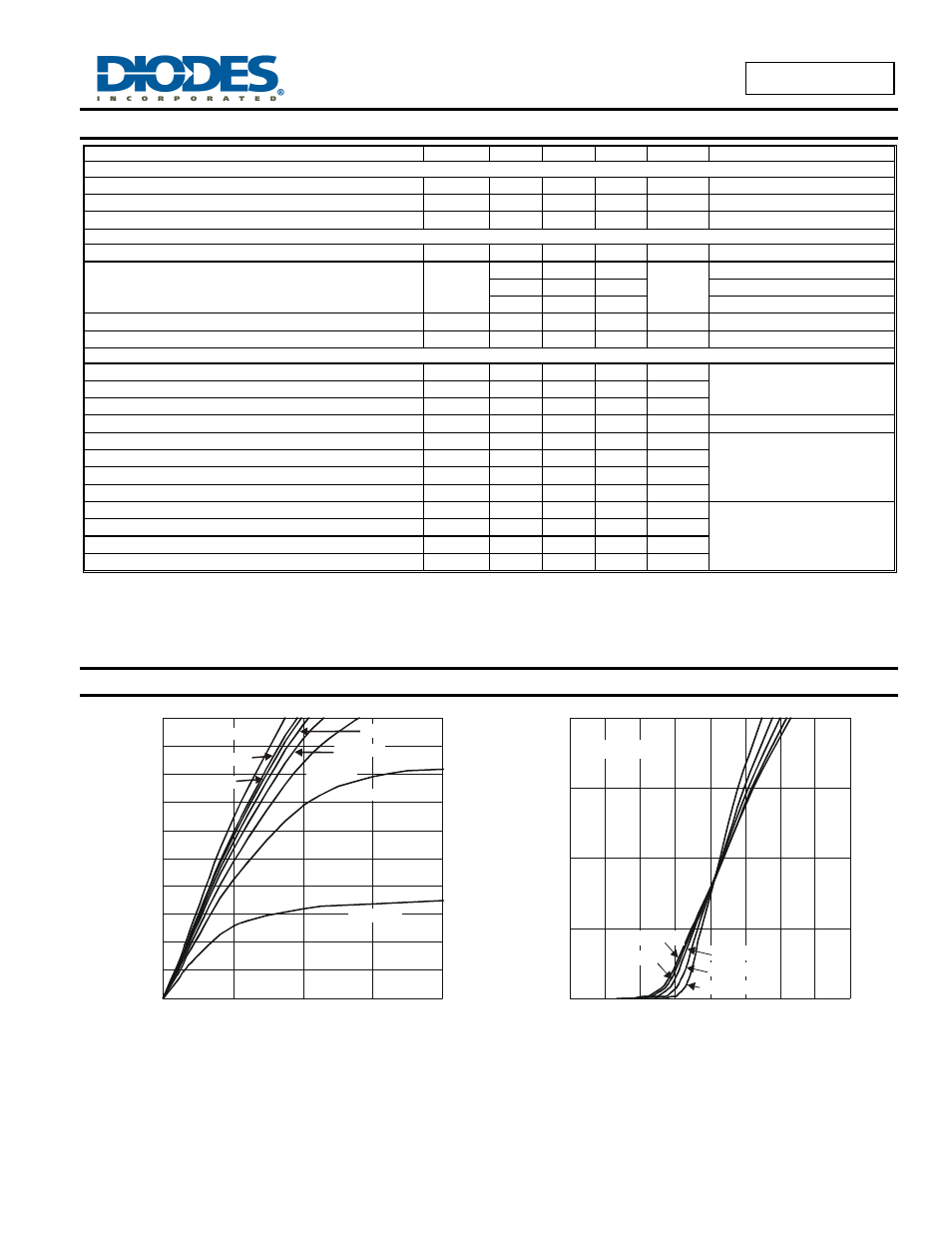
N Channel - Q1
12
16
20
0
0.5
1.0
1.5
2.0
0
4
8
V , DRAIN-SOURCE VOLTAGE (V)
Fig. 1 Typical Output Characteristic
DS
I,
D
R
AI
N
C
U
R
R
E
N
T
(A
)
D
V
= 2.5V
GS
V
= 3.0V
GS
V
= 3.5V
GS
V
= 4.0V
GS
V
= 4.5V
GS
V
= 5.0V
GS
V
= 10V
GS
V
= 2.0V
GS
0
5
10
15
20
0
1
2
3
4
V , GATE-SOURCE VOLTAGE (V)
GS
Fig. 2 Typical Transfer Characteristics
I,
D
R
AI
N
C
U
R
R
ENT (
A
)
D
T = 150°C
A
T = 125°C
A
T = 85°C
A
T = 25°C
A
T = -55°C
A
V
= 5.0V
DS