Dmg6601lvt advance informtion, Maximum ratings, Thermal characteristics – Diodes DMG6601LVT User Manual
Page 2: Electrical characteristics, Q1 and q2, Dmg6601lvt
DMG6601LVT
Document number: DS35405 Rev. 4 - 2
2 of 9
August 2013
© Diodes Incorporated
DMG6601LVT
ADVANCE INFORMTION
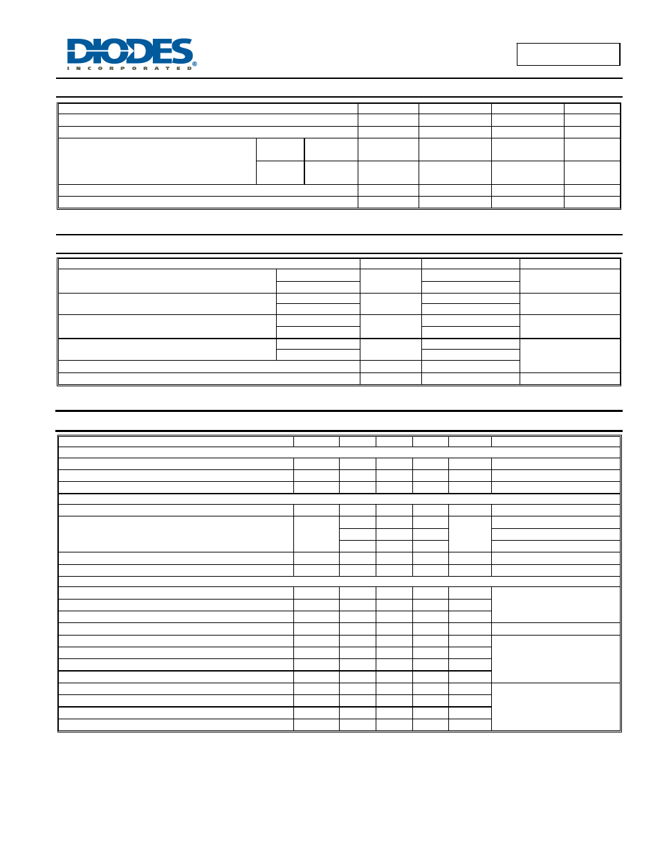
Maximum Ratings
- Q1 and Q2
(@T
A
= +25°C, unless otherwise specified.)
Characteristic Symbol
Q1
Q2
Units
Drain-Source Voltage
V
DSS
30 -30
V
Gate-Source Voltage
V
GSS
±12 ±12 V
Continuous Drain Current (Note 6) V
GS
= 10V
Steady
State
T
A
= +25°C
T
A
= +70°C
I
D
3.8
3.0
-2.5
-2
A
t<10s
T
A
= +25°C
T
A
= +70°C
I
D
4.5
3.4
-3
-2.3
A
Maximum Body Diode Forward Current (Note 6)
I
S
1.5 -1.5
A
Pulsed Drain Current (Note 6)
I
DM
20 -15
A
Thermal Characteristics
(@T
A
= +25°C, unless otherwise specified.)
Characteristic Symbol
Value
Units
Total Power Dissipation (Note 5)
T
A
= +25°C
P
D
0.85
W
T
A
= +70°C
0.54
Thermal Resistance, Junction to Ambient (Note 5)
Steady state
R
JA
147
°C/W
t<10s 103
Total Power Dissipation (Note 6)
T
A
= +25°C
P
D
1.3
W
T
A
= +70°C
0.83
Thermal Resistance, Junction to Ambient (Note 6)
Steady state
R
JA
96
°C/W
t<10s 67
Thermal Resistance, Junction to Case (Note 6)
R
JC
36
Operating and Storage Temperature Range
T
J,
T
STG
-55 to +150
°C
Electrical Characteristics
-
Q1
(@T
A
= +25°C, unless otherwise specified.)
Characteristic
Symbol
Min
Typ
Max
Unit
Test Condition
OFF CHARACTERISTICS (Note 7)
Drain-Source Breakdown Voltage
BV
DSS
30 - - V
V
GS
= 0V, I
D
= 250μA
Zero Gate Voltage Drain Current @T
J
= +25°C
I
DSS
- - 1 μA
V
DS
= 30V, V
GS
= 0V
Gate-Source Leakage
I
GSS
- -
±100
nA
V
GS
= ±12V, V
DS
= 0V
ON CHARACTERISTICS (Note 7)
Gate Threshold Voltage
V
GS(th)
0.5 1 1.5 V
V
DS
= V
GS
, I
D
= 250μA
Static Drain-Source On-Resistance
R
DS (ON)
- 34 55
mΩ
V
GS
= 10V, I
D
= 3.4A
- 38 65
V
GS
= 4.5V, I
D
= 3A
49 85
V
GS
= 2.5V, I
D
= 2A
Forward Transfer Admittance
|Y
fs
|
- 6 - S
V
DS
= 5V, I
D
= 3.4A
Diode Forward Voltage (Note 7)
V
SD
- 0.75 1.0 V
V
GS
= 0V, I
S
= 1A
DYNAMIC CHARACTERISTICS (Note 8)
Input Capacitance
C
iss
- 422 - pF
V
DS
= 15V, V
GS
= 0V,
f = 1.0MHz
Output Capacitance
C
oss
- 41 - pF
Reverse Transfer Capacitance
C
rss
- 39 - pF
Gate resistance
R
g
1.26 - Ω
V
DS
= 0V, V
GS
= 0V, f = 1.0MHz
Total Gate Charge (V
GS
= 4.5V)
Q
g
- 5.4 - nC
V
GS
= 10V, V
DS
= 15V,
I
D
= 3.1A
Total Gate Charge (V
GS
= 10V)
Q
g
12.3 - nC
Gate-Source Charge
Q
gs
- 0.8 - nC
Gate-Drain Charge
Q
gd
- 1.2 - nC
Turn-On Delay Time
t
D(on)
- 1.6 - ns
V
DS
= 15V, V
GS
= 10V,
R
L
= 4.7Ω, R
G
=3Ω,
Turn-On Rise Time
t
r
- 7.4 - ns
Turn-Off Delay Time
t
D(off)
- 31.2 - ns
Turn-Off Fall Time
t
f
- 15.6 - ns
Notes:
5. Device mounted on FR-4 substrate PC board, 2oz copper, with minimum recommended pad layout
6. Device mounted on FR-4 substrate PC board, 2oz copper, with thermal vias to bottom layer 1inch square copper plate
7. Short duration pulse test used to minimize self-heating effect.
8. Guaranteed by design. Not subject to product testing.