Electrical characteristics, Dmp2018lfk – Diodes DMP2018LFK User Manual
Page 3
DMP2018LFK
Document number: DS35357 Rev. 5 - 2
3 of 7
March 2012
© Diodes Incorporated
DMP2018LFK
ADVAN
CE I
N
F
O
RM
ATI
O
N
NEW PROD
UC
T
Electrical Characteristics
@ T
A
= 25°C unless otherwise stated
Characteristic
Symbol
Min
Typ
Max
Unit
Test Condition
OFF CHARACTERISTICS (Note 7)
Drain-Source Breakdown Voltage
BV
DSS
-20 - - V
V
GS
= 0V, I
D
= -10mA
Zero Gate Voltage Drain Current T
J
= 25°C
I
DSS
- - -1
μA
V
DS
= -20V, V
GS
= 0V
Gate-Source Leakage
I
GSS
- - ±2
μA
V
GS
= ±10V, V
DS
= 0V
ON CHARACTERISTICS (Note 7)
Gate Threshold Voltage
V
GS(th)
-0.45 - -1.2 V
V
DS
= -10V, I
D
= -200
μA
Static Drain-Source On-Resistance
R
DS (ON)
- 10 16
mΩ
V
GS
= -4.5V, I
D
= -3.6A
- 12 20
V
GS
= -2.5V, I
D
= -3.6A
- 13.6 25
V
GS
= -2.0V, I
D
= -1.8A
- 20 -
V
GS
= -1.5V, I
D
= -1A
Forward Transfer Admittance
|Y
fs
|
10 17 -
S
V
DS
= -10V, I
D
= -3.6A
Diode Forward Voltage
V
SD
- 0.7
1.2 V
V
GS
= 0V, I
S
= -3.6A
DYNAMIC CHARACTERISTICS (Note 8)
Input Capacitance
C
iss
- 4748 -
pF
V
DS
= -10V, V
GS
= 0V,
f = 1.0MHz
Output Capacitance
C
oss
- 833 -
Reverse Transfer Capacitance
C
rss
- 339 -
Gate Resistance
R
g
- 6.2 - Ω
V
DS
= 0V, V
GS
= 0V, f = 1MHz
Total Gate Charge (V
GS
= -10V)
Q
g
- 113 -
nC
V
DS
= -16V, I
D
= -7.2A
Total Gate Charge (V
GS
= -4.5V)
Q
g
- 53 -
Gate-Source Charge
Q
gs
- 7.1 -
Gate-Drain Charge
Q
gd
- 8.5 -
Turn-On Delay Time
t
D(on)
- 22.8 -
ns
V
DD
= -10V, V
GS
= -4.5V,
R
G
= 4.7
Ω, I
D
= -3.6A
Turn-On Rise Time
t
r
- 29.8 -
Turn-Off Delay Time
t
D(off)
- 240.8 -
Turn-Off Fall Time
t
f
- 100.6 -
Notes:
6. UIS in production with L = 0.5mH, TJ = 25°C
7 .Short duration pulse test used to minimize self-heating effect.
8. Guaranteed by design. Not subject to production testing.
0
0.5
1
1.5
2
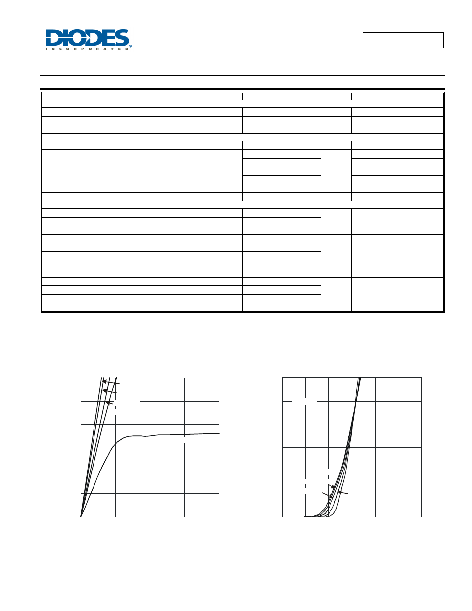
Fig. 1 Typical Output Characteristic
-V
, DRAIN-SOURCE VOLTAGE (V)
DS
0
5
10
15
20
25
30
-I
, D
R
AI
N
C
U
R
R
EN
T
(A
)
D
V
= -1.5V
GS
V
= -2.0V
GS
V
= -2.5V
GS
V
= -4.5V
GS
V
= -10V
GS
0
0.5
1
1.5
2
2.5
3
Fig. 2 Typical Transfer Characteristic
-V
, GATE-SOURCE VOLTAGE (V)
GS
0
5
10
15
20
25
30
-I
, D
R
AI
N
C
U
R
R
EN
T
(A)
D
T = -55°C
A
T = 25°C
A
T = 85°C
A
T = 125°C
A
T = 150°C
A
V
= -5V
DS