Maximum ratings, Thermal characteristics – Diodes DMP2018LFK User Manual
Page 2
DMP2018LFK
Document number: DS35357 Rev. 5 - 2
2 of 7
March 2012
© Diodes Incorporated
DMP2018LFK
ADVAN
CE I
N
F
O
RM
ATI
O
N
NEW PROD
UC
T
Maximum Ratings
@T
A
= 25°C unless otherwise specified
Characteristic Symbol
Value
Units
Drain-Source Voltage
V
DSS
-20 V
Gate-Source Voltage
V
GSS
±12 V
Continuous Drain Current (Note 5) V
GS
= -4.5V
Steady
State
T
A
= 25
°C
T
A
= 70
°C
I
D
-9.2
-7.3
A
t<5s
T
A
= 25
°C
T
A
= 70
°C
I
D
-12.8
-10.3
A
Continuous Drain Current (Note 5) V
GS
= -2.0V
Steady
State
T
A
= 25
°C
T
A
= 70
°C
I
D
-7.1
-6
A
t<5s
T
A
= 25
°C
T
A
= 70
°C
I
D
-10
-8.3
A
Maximum Continuous Body Diode Forward Current (Note 5)
I
S
-3 A
Pulsed Drain Current (10
μs pulse, duty cycle = 1%)
I
DM
-90 A
Avalanche Current (Note 6)
I
AS
17 A
Repetitive Avalanche Energy (Note 6)
E
AS
72 mJ
Thermal Characteristics
Characteristic Symbol
Value
Units
Total Power Dissipation (Note 4)
T
A
= 25°C
P
D
1
W
T
A
= 70°C
0.63
Thermal Resistance, Junction to Ambient (Note 4)
Steady State
R
θJA
126
°C/W
t<5s 60
Total Power Dissipation (Note 5)
T
A
= 25°C
P
D
2.1
W
T
A
= 70°C
1.3
Thermal Resistance, Junction to Ambient (Note 5)
Steady State
R
θJA
61
°C/W
t<5s 29
Thermal Resistance, Junction to Case
R
θJC
6.4
Operating and Storage Temperature Range
T
J,
T
STG
-55 to 150
°C
Notes:
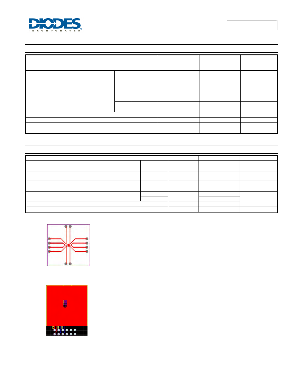
4. Device mounted on FR-4 PC board, with minimum recommended pad layout, single sided.
Notes:
5. Device mounted on FR-4 substrate PC board, 2oz copper, with thermal vias to bottom layer 1inch square copper plate