Diodes DMP2018LFK User Manual
Product summary, Description and applications, Features and benefits
DMP2018LFK
Document number: DS35357 Rev. 5 - 2
1 of 7
March 2012
© Diodes Incorporated
DMP2018LFK
ADVAN
CE I
N
F
O
RM
ATI
O
N
NEW PROD
UC
T
P-CHANNEL ENHANCEMENT MODE MOSFET
Product Summary
V
(BR)DSS
R
DS(on)max
I
D
T
A
= 25°C
-20V
16m
Ω @ V
GS
= -4.5V
-12.8A
25m
Ω @ V
GS
= -2.0V
-10A
Description and Applications
This new generation MOSFET has been designed to minimize the on-
state resistance (R
DS(on)
) and yet maintain superior switching
performance, making it ideal for high efficiency power management
applications.
• DC-DC
Converters
•
Power management functions
•
Notebook PC Applications
•
Portable Equipment Applications
Features and Benefits
• Low
On-Resistance
•
Low Input Capacitance
•
Low Input/Output Leakage
•
ESD Protected Gate up to 2kV
•
Lead Free by Design, RoHS Compliant (Note 1)
•
"Green" Device (Note 2)
•
Qualified to AEC-Q101 Standards for High Reliability
Mechanical Data
• Case:
U-DFN2523-6
•
Case Material: Molded Plastic, "Green" Molding Compound.
UL Flammability Classification Rating 94V-0
•
Moisture Sensitivity: Level 1 per J-STD-020
• Terminals:
Finish
⎯ NiPdAu over Copper leadframe. Solderable
per MIL-STD-202, Method 208
•
Weight: 0.008 grams (approximate)
Ordering Information
(Note 3)
Part Number
Case
Packaging
DMP2018LFK-7
U-DFN2523-6
3,000 / Tape & Reel
DMP2018LFK-13
U-DFN2523-6
10,000 / Tape & Reel
Notes:
1. EU Directive 2002/95/EC (RoHS) & 2011/65/EU (RoHS 2) compliant. No purposely added lead. Halogen and Antimony free.
2. Diodes Inc.'s "Green" policy can be found on our w3. For packaging details, go to our website at
Marking Information
Date Code Key
Year
2011
2012
2013
2014
2015
2016
2017
Code Y
Z
A
B
C D
E
Month
Jan
Feb
Mar
Apr
May
Jun
Jul
Aug
Sep
Oct
Nov
Dec
Code 1 2 3 4 5 6 7 8 9 O N D
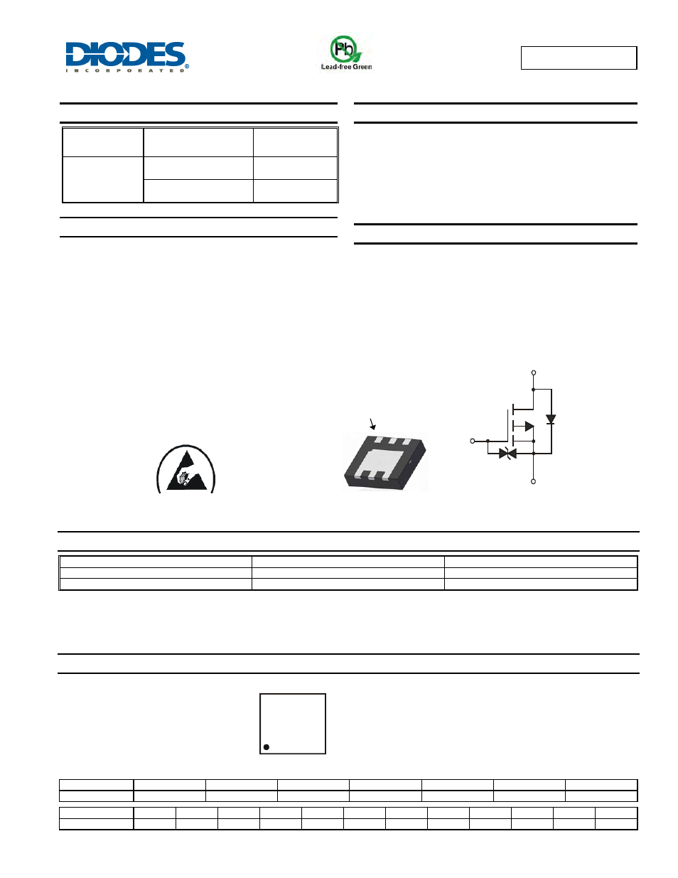
U-DFN2523-6
Bottom View
Equivalent Circuit
P8 = Product Type Marking Code
YM = Date Code Marking
Y = Year (ex: Y = 2011)
M = Month (ex: 9 = September)
Source
Gate
Protection
Diode
Gate
Drain
ESD PROTECTED TO 2kV
Pin 1, 2 = Source
Pin 3 = Gate
Pin 4, 5, 6 = Drain
P8
YM
Pin 1