Single 3 input positive nand gate, New prod uc t electrical characteristics, Package characteristics – Diodes 74LVC1G10 User Manual
Page 5
74LVC1G10
SINGLE 3 INPUT POSITIVE NAND GATE
74LVC1G10
Document number: DS35121 Rev. 3 - 2
5 of 13
October 2011
© Diodes Incorporated
NEW PROD
UC
T
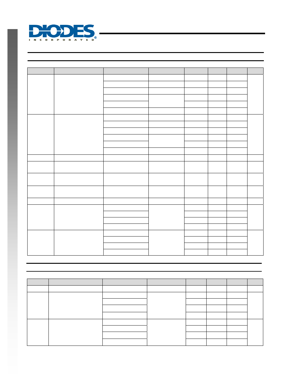
Electrical Characteristics
T
A
= -40
°C to 125°C (All typical values are at V
CC
= 3.3V, T
A
= 25°C)
Symbol
Parameter
Test Conditions
V
CC
Min
Typ.
Max
Unit
V
OH
High Level Output
Voltage
I
OH
= -100
μA
1.65V to 5.5V
V
CC
– 0.1
V
I
OH
= -4mA
1.65V 0.95
I
OH
= -8mA
2.3V 1.7
I
OH
= -16mA
3V
1.9
I
OH
= -24mA
2.0
I
OH
= -32mA
4.5V 3.4
V
OL
High-level Input Voltage
I
OL
= 100
μA
1.65V to 5.5V
0.1
V
I
OL
= 4mA
1.65V
0.70
I
OL
= 8mA
2.3V
0.45
I
OL
= 16mA
3V
0.60
I
OL
= 24mA
0.80
I
OL
= 32mA
4.5V
0.80
I
I
Input Current
V
I
= 5.5 V or GND
0 to 5.5V
± 20
μA
I
OFF
Power Down Leakage
Current
V
I
or V
O
= 5.5V
0
± 20
μA
I
CC
Supply Current
V
I
= 5.5V of GND
I
O
=0
1.65V to 5.5V
40
μA
ΔI
CC
Additional Supply
Current
Input at V
CC
–0.6V
3V to 5.5V
5000
μA
C
i
Input Capacitance
V
i
= V
CC
– or GND
3.3
4
pF
θ
JA
Thermal Resistance
Junction-to-Ambient
SOT26
(Note 4)
204
o
C/W
SOT363
371
DFN1410
430
DFN1010
510
θ
JC
Thermal Resistance
Junction-to-Case
SOT26
(Note 4)
52
o
C/W
SOT363
143
DFN1410
190
DFN1010
250
Package Characteristics (
All typical values are at Vcc = 3.3V, T
A
= 25°C)
Symbol
Parameter
Test Conditions
V
CC
Min
Typ.
Max
Unit
C
I
Input Capacitance
V
I
= V
CC
– or GND
3.3
3.5
pF
θ
JA
Thermal Resistance
Junction-to-Ambient
SOT26
(Note 4)
204
o
C/W
SOT363
371
DFN1410
430
DFN1010
510
θ
JC
Thermal Resistance
Junction-to-Case
SOT26
(Note 4)
52
o
C/W
SOT363
143
DFN1410
190
DFN1010
250
Notes: 4. Test condition for SOT26, SOT363, DFN1410 and DFN1010 : Device mounted on FR-4 substrate PC board, 2oz copper, with minimum
recommended pad layout.