Single 3 input positive nand gate, New prod uc t pin descriptions, Logic diagram – Diodes 74LVC1G10 User Manual
Page 2: Function table, Absolute maximum ratings
74LVC1G10
SINGLE 3 INPUT POSITIVE NAND GATE
74LVC1G10
Document number: DS35121 Rev. 3 - 2
2 of 13
October 2011
© Diodes Incorporated
NEW PROD
UC
T
Pin Descriptions
Pin Name
Description
A Data
Input
GND Ground
B Data
Input
Y Data
Output
V
CC
Supply Voltage
C Data
Input
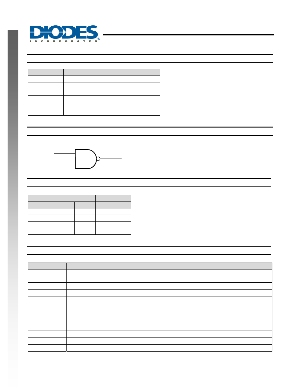
Logic Diagram
Function Table
Inputs
Output
A
B
C
Y
H H H
L
L X X
H
X L X
H
X X L
H
Absolute Maximum Ratings
(Note 2)
Symbol
Description
Rating
Unit
ESD HBM
Human Body Model ESD Protection
2
KV
ESD MM
Machine Model ESD Protection
200
V
V
CC
Supply Voltage Range
-0.5 to 6.5
V
V
I
Input Voltage Range
-0.5 to 6.5
V
V
O
Voltage applied to output in high impedance or I
OFF
state
-0.5 to 6.5
V
V
O
Voltage applied to output in high or low state
-0.3 to V
CC
+0.5
V
I
IK
Input Clamp Current V
I
<0
-50 mA
I
OK
Output Clamp Current
-50
mA
I
O
Continuous output current
±50
mA
Continuous current through Vdd or GND
±100
mA
T
J
Operating Junction Temperature
-40 to 150
°C
T
STG
Storage Temperature
-65 to 150
°C
Notes: 2. Stresses beyond the absolute maximum may result in immediate failure or reduced reliability. These are stress values and device
operation should be within recommend values.
A
3
4
Y
B
6
C
1