Data sheet, Functional block diagram – Diodes AP3606/AP3607 User Manual
Page 3
Data Sheet
4/6 CHANNEL CHARGE PUMP CURRENT SINK FOR LED DRIVER AP3606/AP3607
Jan. 2013 Rev. 1. 5 BCD Semiconductor Manufacturing Limited
3
PGND
AGND
VOUT1
VOUT2
VIN
EN
C1-
C1+
C2-
C2+
D2
D1
D3
D4
1x/1.5x Charge Pump
1MHz
OSC
Current Limitation
Soft Start
OTSD
UVLO
OVP
4 Channels Current Sink
16 Steps Pulse
Dimming Controller
Shutdown
Delay
1
4
3
2
5
6
7
8
10
11
12
13
14
16
1x /1.5x Charge Pump
1MHz
OSC
Shutdown
Delay
16 Steps Pulse
Dimming Controller
Current Limitation
Soft Start
OVP
UVLO
PGND
AGND
VOUT1
VOUT2
VIN
EN
OTSD
D2 D3 D4 D5
D6
1
2
3
4
5
6
7
8
9
10
11
12
13
14
15
16
C1- C1+
C2-
C2+
D1
6 Channels Current Sink
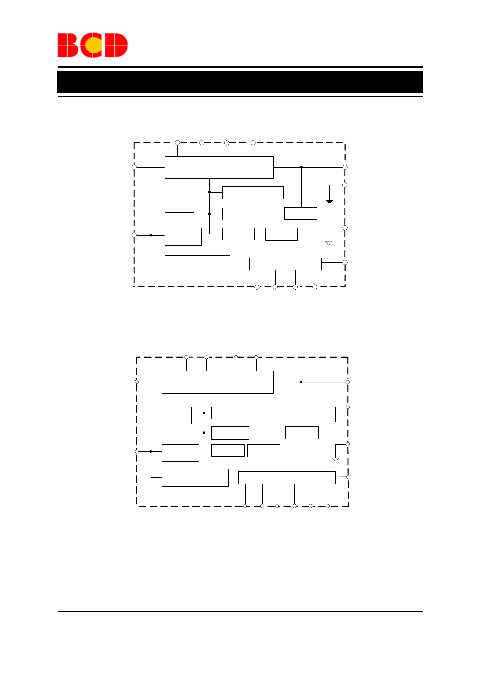
Functional Block Diagram
AP3606
AP3607
Figure 3. Functional Block Diagram of AP3606/AP3607
See also other documents in the category Diodes Hardware:
- PDS3200 (5 pages)
- PDS340 (5 pages)
- PDS340Q (5 pages)
- PDS360 (5 pages)
- PDS360Q (5 pages)
- PDS4150 (4 pages)
- PDS3100Q (5 pages)
- PDS3100 (5 pages)
- PDS1240CTL (5 pages)
- PDS1045 (5 pages)
- PDS1040L (5 pages)
- PDS1040CTL (5 pages)
- PDS1040 (5 pages)
- PD3S230L (5 pages)
- PD3S230H (3 pages)
- PDS5100Q (5 pages)
- PDS835L (5 pages)
- PDS760 (5 pages)
- PDS560 (5 pages)
- PDS540 (5 pages)
- PDS5100H (5 pages)
- PDS5100 (5 pages)
- PDS4200H (6 pages)
- SBL3060CTP (4 pages)
- SBL30L30CT (3 pages)
- SBL3045CTP (4 pages)
- SBL3040CTP (4 pages)
- SBL2060CTP (4 pages)
- SBL2030CT - SBL2060CT (3 pages)
- SBL2045CTP (4 pages)
- SBL1060CTP (4 pages)
- SBL1040CTP (4 pages)
- SBG3030CT - SBG3045CT (5 pages)
- SB520 - SB560 (3 pages)
- SB370 - SB3100 (3 pages)
- SB320 - SB360 (3 pages)
- SBR10U100CT (5 pages)
- SBR10U150CT (5 pages)
- SBR10A45SP5 (5 pages)
- SBR1060CT (5 pages)
- SBR1045SP5 (5 pages)
- SBR1045SD1 (4 pages)
- SBR1045D1 (5 pages)
- SBR1045CTL (4 pages)
- SBR1040CT (5 pages)