Data sheet, Pin configuration, Pin description – Diodes AP3606/AP3607 User Manual
Page 2: Fn package (qfn-3×3-16)
Data Sheet
4/6 CHANNEL CHARGE PUMP CURRENT SINK FOR LED DRIVER AP3606/AP3607
Jan. 2013 Rev. 1. 5 BCD Semiconductor Manufacturing Limited
2
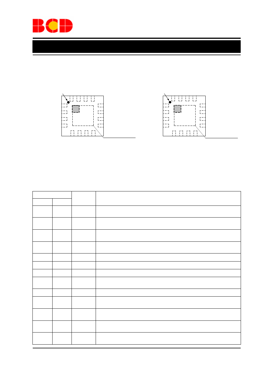
Pin Configuration
FN Package
(QFN-3×3-16)
AP3606 AP3607
Figure 2. Pin Configuration of AP3606/AP3607 (Top View)
Pin Description
Pin Number
Pin Name
Function
AP3606 AP3607
1 1 C1-
Flying capacitor 1 negative terminal. The flying capacitor should be connected as
close to this pin as possible
2 2 C2-
Flying capacitor 2 negative terminal. The flying capacitor should be connected as
close to this pin as possible
3 3 C2+
Flying capacitor 2 positive terminal. The flying capacitor should be connected as
close to this pin as possible
4 4 C1+
Flying capacitor 1 positive terminal. The flying capacitor should be connected as
close to this pin as possible
5 5
AGND
Analog
ground
6 6
PGND
Power
ground
7 7 VIN
Supply
voltage
input
8 8 EN
Enable control input. Logic high enables the IC; while logic low forces the IC into
shutdown mode. It is used for digital dimming by applying a pulse signal on it.
9, 15
NC
No connection (AP3606 only)
9, 10
D6 , D5
Current sink for WLED6 and WLED5. Connect the cathode of WLEDs to these
pins. If not used, these pins must be connected with VIN (AP3607 only)
10, 11, 12,
13
11, 12, 13,
14
D4 ~ D1
Current sink for WLED4, 3, 2, 1. Connect the cathode of WLEDs to these pins. If
not used, these pins must be connected with VIN
14 15
VOUT2
Output pin 2. It powers 4 channels current sink (AP3606) and 6 channels current
sink (AP3607)
16 16
VOUT1
Output Pin 1. It’s the charge pump output. The output capacitor should be placed
closely to this pin
E P
5
6
7
8
1
2
3
4
9
12
Pin 1 Mark
11
10
13
14
15
16
C1-
C1+
C2+
C2-
NC
D4
D3
D2
D1
NC
VO
U
T
1
VOUT
2
AG
N
D
PG
N
D
VI
N
EN
Note: Pin 14 should be connected with Pin 16 on PCB Board.
Exposed PAD,
Connected to AGND
E P
5
6
7
8
1
2
3
4
9
12
Pin 1 Mark
11
10
13
14
15
16
C1-
C1+
C2+
C2-
D5
D4
D3
D2
VO
U
T
1
VO
UT
2
AG
N
D
PG
N
D
VI
N
EN
Note: Pin 15 should be connected with Pin 16 on PCB Board.
Exposed PAD,
Connected to AGND
D1
D6