Recommended operating conditions, Electrical characteristics, Ap8800a – Diodes AP8800A User Manual
Page 3
AP8800A
Document number: DS35100 Rev. 3 - 2
3 of 13
August 2012
© Diodes Incorporated
AP8800A
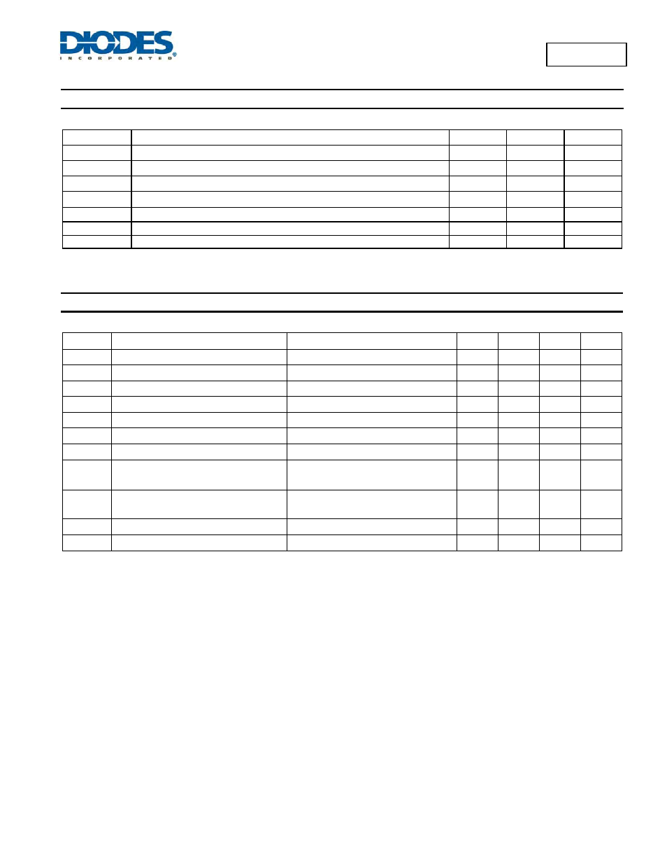
Recommended Operating Conditions
(@T
A
= +25°C, unless otherwise specified.)
Symbol Parameter Min
Max
Unit
V
IN
Operating Input Voltage Relative to GND
8.0
28
V
V
CTRLDC
Voltage Range for 24% to 200% DC Dimming Relative to GND
0.3
2.5
V
V
CTRLL
Voltage Low for PWM Dimming Relative to GND
0.2
V
I
SW
Continuous Average Switch Current (Note 4)
370
mA
D
PWM
Duty Cycle Range Applied to CTRL (f < 500Hz)
0.01
1
f
SW
Switching
Frequency
600
kHz
T
A
Ambient Temperature Range
-40
105
°C
Note:
4. Dependent on junction and ambient temperature.
Electrical Characteristics
(@T
A
= +25°C, V
IN
= 12V, unless otherwise specified.)
Symbol Parameter
Conditions Min
Typ
Max
Unit
I
Q
Quiescent
Current
V
CTRL
= 1.25V, f
SW
= 250kHz
300
650
µA
I
SD
Shutdown
Current
V
CTRL
= 0V
20
30
µA
V
THD
Internal Threshold Voltage
95
100
105
mV
V
REF
Internal Reference Voltage
1.25
V
I
SET
SET Pin Input Current
V
SET
= V
IN
-0.1
1.3 µA
R
DS(ON)
On Resistance of MOSFET
1.5
2.2
Ω
I
SW-LKG
Switch
Leakage
Current
5
µA
f
SW
Switching Frequency with L = 100µH
ADJ pin floating L = 100H
I
OUT
= 350mA @ 1 LED (V
LED
= 3.4V)
250 kHz
t
SS
Soft-Start
Time
Time taken for output current to reach 90%
of final value after V
CTRL
= 0.3V
500 µs
t
PD
Internal Comparator Propagation Delay
55
ns
θ
JA
Thermal Resistance Junction-to-Ambient
TSOT25 (Note 5)
200
°C/W
Note:
5. Test condition for TSOT25: Device mounted on FR-4 PCB (25mm x 25mm 1oz copper, minimum recommended pad layout on
top layer and thermal vias to bottom layer ground plane. For better thermal performance, larger copper pad for heat-sink is needed.