Az2085 – Diodes AZ2085 User Manual
Page 5
AZ2085
Document number: DS36595 Rev.
3 - 2
5 of 11
March 2014
© Diodes Incorporated
AZ2085
A Product Line of
Diodes Incorporated
N
E
W
P
R
O
D
U
C
T
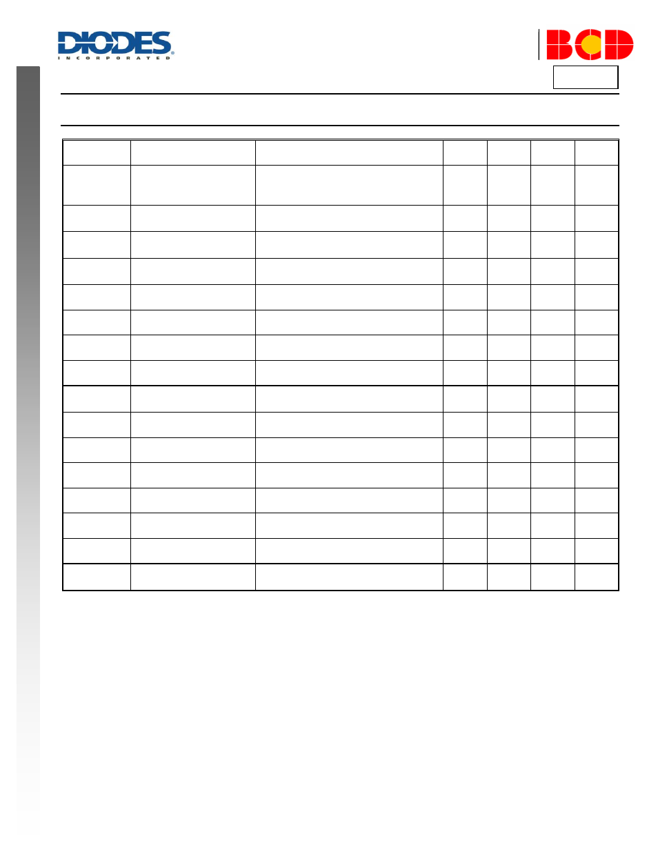
Electrical Characteristics
(Typicals and limits appearing in normal type apply for T
J
= +25ºC. Limits appearing in Boldface type
apply over the entire operating junction temperature range 0 to +125ºC.)
Symbol
Parameter
Conditions
Min
Typ
Max
Unit
V
REF
Reference Voltage
I
OUT
= 10mA, V
IN
-V
OUT
= 3V, T
J
= +25°C,
10mA
≤ I
OUT
≤ 3A,
1.5V
≤ V
IN
-V
OUT
≤ 5V
1.238
1.225
1.250
1.250
1.262
1.275
V
ΔV
OUT
/V
OUT
Load Regulation
0A
≤ I
OUT
≤ 3A, V
IN
-V
OUT
= 3V
—
0.1
0.2
0.3
0.4
%
ΔV
OUT
/
ΔV
IN
Line Regulation
I
OUT
= 10mA,
2.85V
≤ V
IN
≤ 10V
—
0.015
0.035
0.2
0.2
%
V
DROP
Dropout Voltage
I
OUT
= 3A,
ΔV
REF
,
ΔV
OUT
= 1%
—
1.2
1.5
V
I
LIMIT
Current Limit
V
IN
-V
OUT
= 3V
3.2
4.5
—
A
I
LOAD
Minimum Load Current
V
IN
= 10V
—
0.3
1
mA
I
ADJ
Adjust Pin Current
V
IN
= 4.25V, I
OUT
= 10mA
—
6
10
μA
ΔI
ADJ
Adjust Pin Current Change
10mA
≤ I
OUT
≤ 3A, 1.5V ≤ V
IN
-V
OUT
≤ 6V
—
0.3
2
μA
PSRR
Ripple Rejection
f
RIPPLE
= 120Hz, C
OUT
= 22
μF, I
OUT
= 3A,
V
IN
-V
OUT
= 3V
—
72
—
dB
—
Long Term Stability
T
A
= +125°C, 1000Hrs
—
0.5
—
%
—
Temperature Stability
I
OUT
= 10mA, V
IN
-V
OUT
= 1.5V
—
0.5
—
%
—
RMS Noise (% of V
OUT
)
T
A
= +125°C, 10Hz
≤ f ≤ 10kHz
—
0.003
—
%
—
OTSD
—
+130
+150
+170
°C
—
OTSD Hysteresis
—
—
+20
—
°C
—
Pulse Current
Pulse Width
≤ 100μS
—
7
12
A
θ
JC
Thermal Resistance
(Junction to Case)
—
—
7.36
—
°C/W