Ap7365, New prod uc t, Electrical characteristics – Diodes AP7365 User Manual
Page 4
AP7365
600mA, LOW QUIESCENT CURRENT, FAST TRANSIENT
LOW DROPOUT LINEAR REGULATOR
AP7365
Document number: DS32260 Rev. 3 - 2
4 of 19
May 2012
© Diodes Incorporated
NEW PROD
UC
T
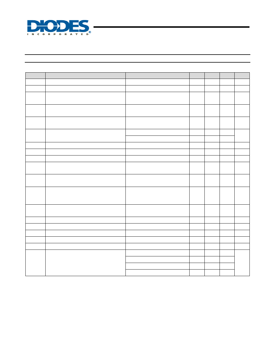
Electrical Characteristics
(T
A
= +25°C, V
IN
= V
OUT
+1V, C
IN
= 1
μF, C
OUT
= 1
μF, V
EN
= 2V, unless otherwise stated)
Symbol
Parameter
Test Conditions
Min
Typ
Max
Unit
V
REF
ADJ Reference Voltage (Adjustable version)
I
OUT
= 0mA
0.8 V
I
ADJ
ADJ Leakage (Adjustable version)
0.1
1.0
μA
V
OUT
Output Voltage Accuracy
T
A
= -40°C to +85°C,
I
OUT
= 10% of I
OUT-Max
-2 +2
%
ΔV
OUT
/
ΔV
IN
/V
Line Regulation
V
IN
= (V
OUT
+1V) to V
IN-Max
,
V
EN
= V
IN
, I
OUT
= 1mA
0.02
0.20
%/V
ΔV
OUT
/V
OUT
Load Regulation
V
IN
= (V
OUT
+1V) to V
IN-Max
,
I
OUT
= 1mA to 600mA
-1.0 +1.0
%
V
DROPOUT
Dropout Voltage (Note 5)
V
OUT
< 2.5V, I
OUT
= 600mA
370
600
mV
V
OUT
≥ 2.5V, I
OUT
= 600mA
300
400
I
Q
Input Quiescent Current
V
EN
= V
IN
, I
OUT
= 0mA
35
80
μA
I
SHDN
Input Shutdown Current
V
EN
= 0V, I
OUT
= 0mA
0.1
1.0
μA
I
LEAK
Input Leakage Current
V
EN
= 0V, OUT grounded
0.1
1.0
μA
t
ST
Start-up Time
V
EN
= 0V to 2.0V in 1
μs,
I
OUT
= 600mA
200
μs
PSRR
PSRR (Note 6)
V
IN
= [V
OUT
+1V] V
DC
+ 0.5V
ppAC
,
f = 1kHz, I
OUT
= 50mA
65 dB
I
SHORT
Short-circuit Current
V
IN
= V
IN-Min
to V
IN-Max
,
V
OUT
< 0.2V (fixed version) or 25% of
V
OUT
(ADJ version)
240 mA
I
LIMIT
Current limit
V
IN
= V
IN-Min
to V
IN-Max
,
V
OUT
/R
OUT
= 2.5A
0.8 1.4
A
V
IL
EN Input Logic Low Voltage
V
IN
= V
IN-Min
to V
IN-Max
0.4
V
V
IH
EN Input Logic High Voltage
V
IN
= V
IN-Min
to V
IN-Max
1.4 V
I
EN
EN Input Current
V
IN
= 0V or V
IN-Max
-1 +1
μA
T
SHDN
Thermal shutdown threshold
145
°C
T
HYS
Thermal shutdown hysteresis
15
°C
θ
JA
Thermal Resistance Junction-to-Ambient
SOT25 (Note 7)
187
o
C/W
U-DFN2020-6 (Note 7)
251
SOT89-3 (Note 7)
141
SOT223 (Note 7)
153
Notes:
5. Dropout voltage is the voltage difference between the input and the output at which the output voltage drops 2% below its nominal value. This
parameter only applies to input voltages above minimum V
IN
= 2.0V.
6. At V
IN
< 2.3V, the PSRR performance may be reduced.
7. Test condition for all packages: Device mounted on FR-4 substrate PC board, 1oz copper, with minimum recommended pad layout.