Ap7365 – Diodes AP7365 User Manual
Page 10
AP7365
600mA, LOW QUIESCENT CURRENT, FAST TRANSIENT
LOW DROPOUT LINEAR REGULATOR
AP7365
Document number: DS32260 Rev. 3 - 2
10 of 19
May 2012
© Diodes Incorporated
NEW PROD
UC
T
Application Note
Input Capacitor
A 1µF ceramic capacitor is recommended between IN and
GND pins to decouple input power supply glitch and noise. The
amount of the capacitance may be increased without limit. This
input capacitor must be located as close as possible to the device
to assure input stability and reduce noise. For PCB layout, a wide
copper trace is required for both IN and GND pins. A lower
ESR capacitor type allows the use of less capacitance, while
higher ESR type requires more capacitance.
Output Capacitor
The output capacitor is required to stabilize and improve the
transient response of the LDO. The AP7365 is stable with very
small ceramic output capacitors. Using a ceramic capacitor value
that is at least
1μF with ESR > 15mΩ on the output ensures
stability. Higher capacitance values help to improve line and load
transient response. The output capacitance may be increased to
keep low undershoot and overshoot. Output capacitor must be
placed as close as possible to OUT and GND pins.
Adjustable Operation
The AP7365 provides output voltage from 0.8V to 5.0V through
external resistor divider as shown below.
1uF
IN
G N D
EN
O U T
E nable
A D J
R 2
R 1
1uF
V
IN
V
O U T
A P 7365
The output voltage is calculated by:
⎟⎟
⎠
⎞
⎜⎜
⎝
⎛
+
=
2
R
1
R
1
REF
V
OUT
V
Where V
REF
= 0.8V (the internal reference voltage)
Rearranging the equation will give the following that is used for
adjusting the output to a particular voltage:
⎟⎟
⎠
⎞
⎜⎜
⎝
⎛
−
=
1
REF
V
OUT
V
2
R
1
R
To maintain the stability of the internal reference voltage, R
2
need
to be kept smaller than 80k
Ω.
No Load Stability
Other than external resistor divider, no minimum load is required
to keep the device stable. The device will remain stable and
regulated in no load condition.
ON/OFF Input Operation
The AP7365 is turned on by setting the EN pin high, and is turned
off by pulling it low. If this feature is not used, the EN pin should
be tied to IN pin to keep the regulator output on at all time. To
ensure proper operation, the signal source used to drive the
EN pin must be able to swing above and below the specified
turn-on/off voltage thresholds listed in the Electrical
Characteristics section under V
IL
and V
IH
.
Current Limit Protection
When output current at OUT pin is higher than current limit
threshold, the current limit protection will be triggered and clamp
the output current to approximately 1.4A to prevent over-current
and to protect the regulator from damage due to overheating.
Short Circuit Protection
When OUT pin is short-circuit to GND, short circuit protection will
be triggered and clamp the output current to approximately
240mA. This feature protects the regulator from over-current and
damage due to overheating.
Thermal Shutdown Protection
Thermal protection disables the output when the
junction temperature rises to approximately +145°C, allowing the
device to cool down. When the junction temperature reduces to
approximately +130°C the output
circuitry is enabled again.
Depending on power dissipation, thermal resistance, and ambient
temperature, the thermal protection circuit may cycle on and
off.
This
cycling limits the heat dissipation of the
regulator, protecting it from damage due to overheating.
Ultra Fast Start-Up
After enabled, the AP7365 is able to provide full power in as little
as hundreds of microseconds, typically 200µs, without sacrificing
low ground current. This feature will help load circuitry move in
and out of standby mode in real time, eventually extend battery
life for mobile phones and other portable devices.
300
200
100
0
600
500
400
LOAD CURRENT (mA)
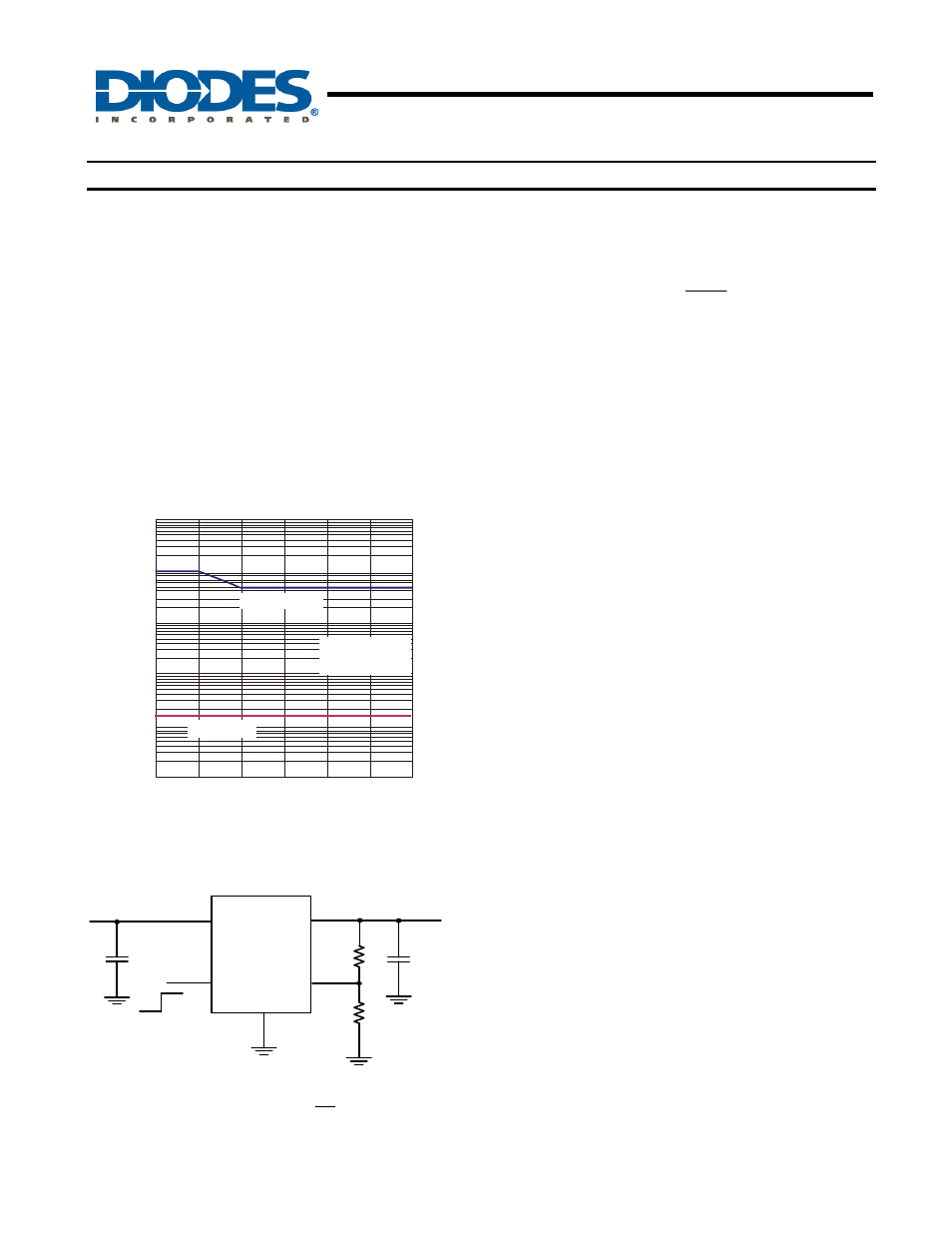
Region of Stable C
ESR vs. Load Current
OUT
100
10
1
0.1
0.01
0.001
C
ESR
(
)
OU
T
Ω
Unstable Range
Stable Range
V = 4.3V
C = C
= 1µF
IN
IN
OUT