Ap7340, Pin descriptions, Functional block diagram – Diodes AP7340 User Manual
Page 2: Absolute maximum ratings, Recommended operating conditions
AP7340
Document number: DS35282 Rev. 3 - 2
2 of 15
February 2014
© Diodes Incorporated
AP7340
Pin Descriptions
Pin Name
PIN No
Function
X2-DFN1010-4
V
OUT
1
Power Output Pin
GND 2
Ground
EN 3
Enable pin. This pin should be driven either high or low and must not be floating. Driving this pin high
enables the regulator, while pulling it low puts the regulator into shutdown mode
V
IN
4
Power Input pin
Thermal
PAD
In PCB layout, prefer to use large copper area to cover this pad for better thermal dissipation, then
connect this area to GND or leave it open. However do not use it as GND electrode function alone.
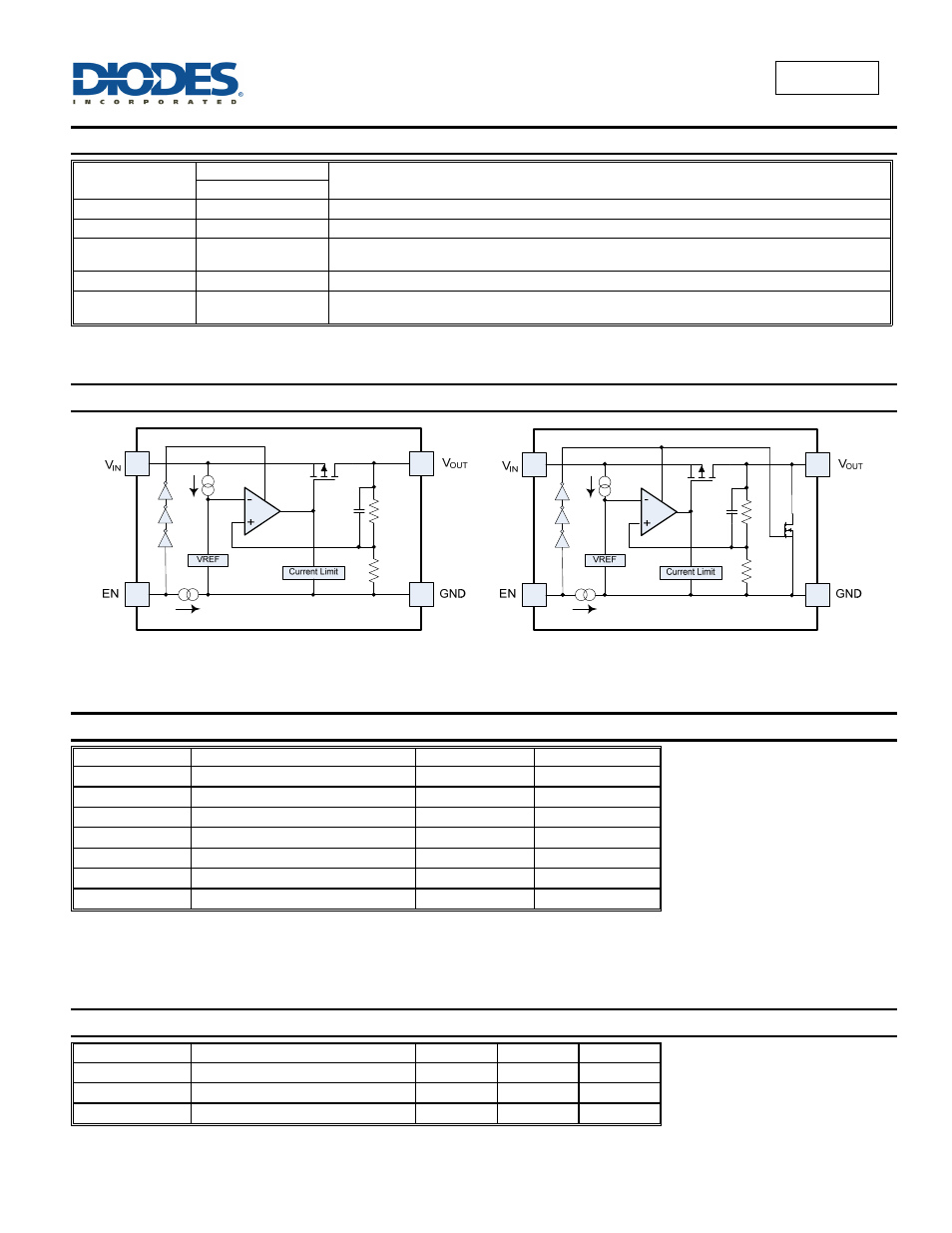
Functional Block Diagram
AP7340 (Non discharge)
AP7340D (with discharge)
Absolute Maximum Ratings
(Note 4) (@T
A
= +25°C, unless otherwise specified.)
Symbol Parameter
Ratings
Unit
V
IN
Input Voltage
6.0
V
V
CE
Input Voltage EN
6.0
V
V
OUT
Output Voltage
-0.3 to V
IN
+0.3
V
I
OUT
Output Current
300
mA
P
D
Power Dissipation
400
mW
T
A
Operating Temperature
-40 to +85
°C
T
STG
Storage Temperature
-55 to +125
°C
Note:
4. a). Stresses beyond those listed under Absolute Maximum Ratings may cause permanent damage to the device. These are stress ratings only and
functional operation of the device at these conditions is not implied. Exposure to absolute-maximum-rated conditions for extended periods may
affect device reliability.
b). Ratings apply to ambient temperature at 25°C . The JEDEC High-K board design used to derive this data was a 2 inch x 2 inch multilayer board
with 1-ounce internal power and ground planes and 2-ounce copper traces on the top and bottom of the board.
Recommended Operating Conditions
(@T
A
= +25°C, unless otherwise specified.)
Symbol
Parameter
Min
Max
Unit
V
IN
Input Voltage
1.7
5.25
V
I
OUT
Output Current
0
150
mA
T
A
Operating Ambient Temperature
-40
+85
°C