Ap7362, Application information – Diodes AP7362 User Manual
Page 9
AP7362
Document number: DS35058 Rev. 6 - 2
9 of 15
August 2013
© Diodes Incorporated
AP7362
Application Information
(cont.)
Stability and Phase Margin
Any regulator which operates using a feedback loop must be compensated in such a way as to ensure adequate phase margin, which is defined
as the difference between the phase shift and -180 degrees at the frequency where the loop gain crosses unity (0 dB). For most LDO regulators,
the ESR of the output capacitor is required to create a zero to add enough phase lead to ensure stable operation. The AP7362 has an internal
compensation circuit which maintains phase margin regardless of the ESR of the output capacitor, any type of capacitor can be used.
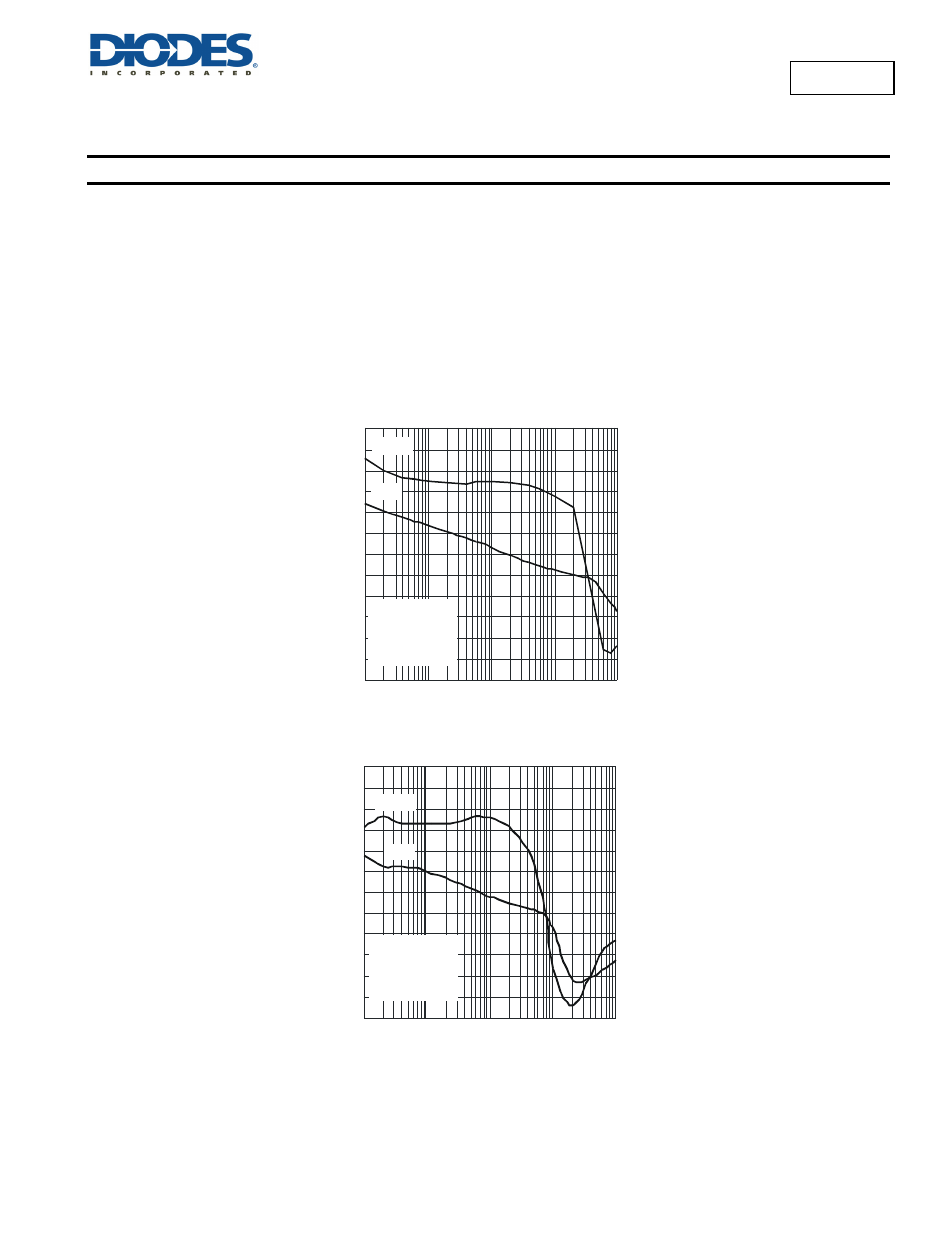
Below two charts show the gain/phase plot of the AP7362 with an output of 1.2V, 10μF ceramic output capacitor, delivering 1.5A load current
and no load. It can be seen the phase margin is about 90° (which is very stable)
.
Below two charts show the gain/phase plot of the AP7362 with an output of 1.2V, 10 μF ceramic output capacitor, delivering 1.5A load current
and no load. It can be seen the phase margin is about 90° (which is very stable)
.
ON/OFF Input Operation
The AP7362 is turned on by setting the EN pin high, and is turned off by pulling it low. If this feature is not used, the EN pin should be tied to IN
pin to keep the regulator output on at all time. To ensure proper operation, the signal source used to drive the EN pin must be able to swing
above and below the specified turn-on/off voltage thresholds listed in the Electrical Characteristics section under V
IL
and V
IH
.
-120
-100
-80
-60
-40
-20
0
20
40
60
80
100
120
FREQUENCY(Hz)
Gain-Bandwidth Plot for 1.5A Load
140
100
120
100
80
60
40
20
0
-20
-40
-60
-80
P
H
ASE M
A
RG
IN
(
°)
1k
10k
100k
1M
PHASE
V = 2.7V
V
= 1.2V
I = 1.5A
C
= 10µF CER
IN
OUT
L
OUT
GAIN
L
O
O
P
G
AI
N (
dB)
-120
-100
-80
-60
-40
-20
0
20
40
60
80
100
120
LO
O
P
G
AI
N
(d
B
)
140
120
100
80
60
40
20
0
-20
-40
-60
-80
P
H
ASE M
A
R
G
IN
(
°)
FREQUENCY(Hz)
Gain-Bandwidth Plot for no Load
100
1k
10k
100k
1M
V = 2.7V
V
= 1.2V
I = 0A
C
= 10µF CER
IN
OUT
L
OUT
PHASE
GAIN