Ap7362, Pin descriptions, Functional block diagram – Diodes AP7362 User Manual
Page 2: Absolute maximum ratings
AP7362
Document number: DS35058 Rev. 6 - 2
2 of 15
August 2013
© Diodes Incorporated
AP7362
Pin Descriptions
Pin Name
Pin Number
Function
GND 1
Ground.
EN
2
Enable input, active high.
IN
3, 4
Voltage input pin.
OUT
5, 6, 7
Voltage output pin.
ADJ 8
Output feedback pin for adjustable version only – a resistor divider from this pin to the OUT pin and
ground sets the output voltage.
NC
8
No connection for fixed output version.
EP EP
The exposed pad (EP) is used to remove heat from the package and it is recommended that it is
connected to a copper area. The die is electrically connected to the exposed pad. It is recommended to
connect it externally to GND, but should not be the only ground connection.
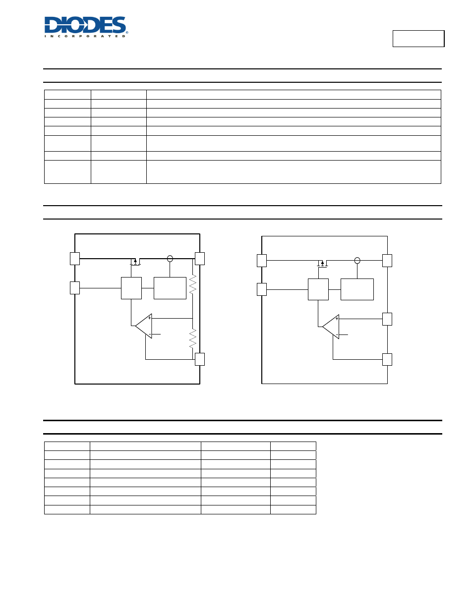
Functional Block Diagram
IN
EN
GND
OUT
Gate
Driver
0.605V
Current Limit
and Thermal
Shutdown
Fixed Version
R
R
IN
EN
GND
ADJ
OUT
Gate
Driver
0.605V
Current Limit
and Thermal
Shutdown
Adjustable Version
Absolute Maximum Ratings
(Note 4)
(@T
A
= +25°C, unless otherwise specified.)
Symbol Parameter
Ratings
Unit
ESD HBM
Human Body Model ESD Protection
2000
V
ESD MM
Machine Model ESD Protection
200
V
V
IN
Input Voltage
-0.3 to +6.0
V
V
OUT
, V
EN
OUT, EN Voltage
-0.3V to V
IN
+0.3
V
I
OUT
Continuous Load Current
Internal Limited
T
ST
Storage Temperature Range
-65 to +150
°C
T
J
Maximum Junction Temperature
150
°C
Note:
4. Stresses beyond those listed under Absolute Maximum Ratings may cause permanent damage to the device. These are stress
Ratings only, and functional operation of the device at these or any other conditions beyond those indicated is not implied.
Exposure to absolute-maximum rated conditions for extended periods may affect device reliability.