Electrical characteristics, Ap7362 – Diodes AP7362 User Manual
Page 4
AP7362
Document number: DS35058 Rev. 6 - 2
4 of 15
August 2013
© Diodes Incorporated
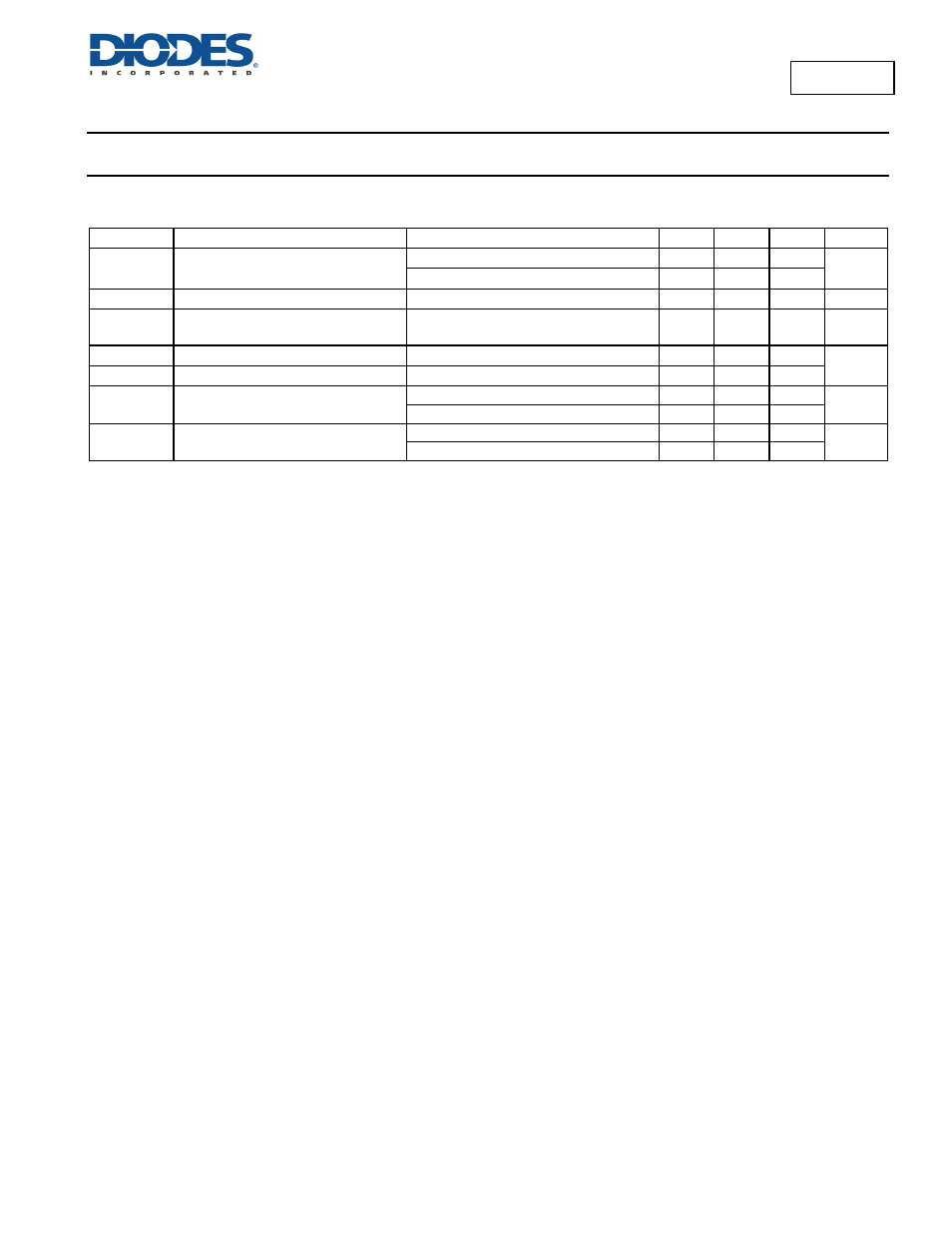
AP7362
Electrical Characteristics
(cont.)
(@T
A
= +25°C, V
IN
= 3.3V, V
OUT
=1.8V, I
OUT
= 10mA, V
EN
= V
IN
, C
IN
= 10μF, C
OUT
= 10μF, V
EN
= 2V, unless otherwise stated.)
Minimum and maximum limits are guaranteed through test, design, or statistical correlation. Typical values represent the most likely parametric
norm at T
A
= +25°C, and are provided for reference purposes only.
Symbol
Parameter Test
Conditions
Min
Typ
Max
Unit
PSRR Ripple
Rejection
V
IN
= 3.0V, I
OUT
= 1.5A, f = 120Hz
65
dB
V
IN
= 3.0V, I
OUT
= 1.5A, f = 1kHz
61
n(l/f)
Output Noise Density
f = 120Hz, C
OUT
= 10μF ceramic
1.0
μV/
Hz
e
n
Output Noise Voltage
BW = 100Hz – 100kHz,
C
OUT
= 10μF ceramic
90
μV(rms)
T
SHDN
Thermal shutdown threshold
T
J
rising
170
C
T
HYS
Thermal shutdown hysteresis
T
J
falling from T
SHDN
10
θ
JA
Thermal Resistance Junction-to-Ambient
U-DFN2030-8 (Note 8)
85.0
°C/W
SO-8EP (Note 8)
52.8
θ
JC
Thermal Resistance Junction-to-Case
U-DFN2030-8 (Note 8)
17.0
°C/W
SO-8EP (Note 8)
10.0
Note:
8. Device mounted on 2” x 2” FR-4 substrate PCB, 2oz copper with minimum recommended pad layout.