Ap7115, Electrical characteristics, 150ma low dropout linear regulator with shutdown – Diodes AP7115 User Manual
Page 4

AP7115
150mA LOW DROPOUT LINEAR REGULATOR WITH
SHUTDOWN
AP7115 Rev. 10
4 of 11
MAY 2009
©
Diodes Incorporated
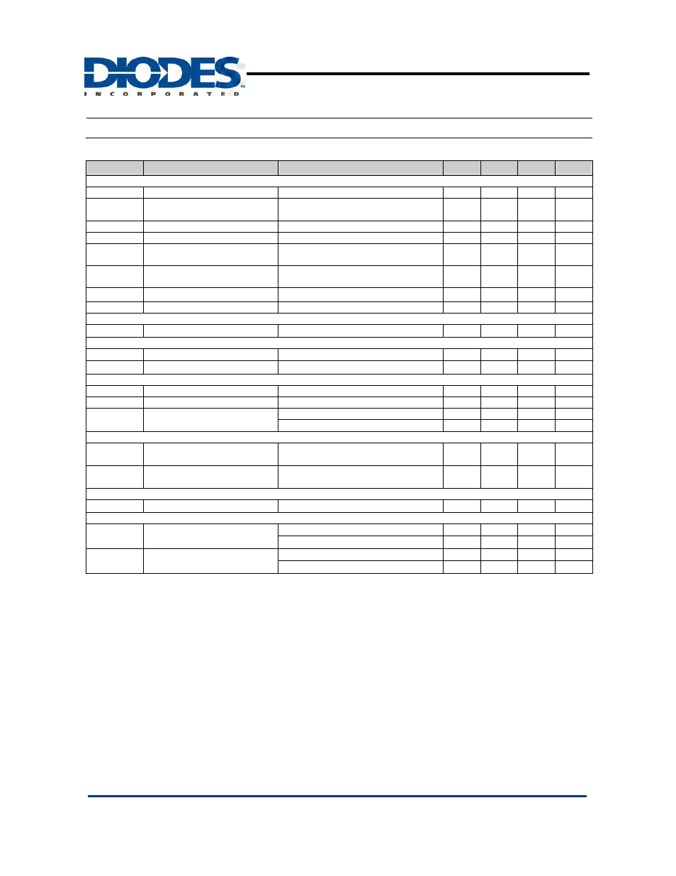
Electrical Characteristics
(V
CC
= 3.3V, I
L
= 30mA, C
IN
= 1
μF, C
OUT
= 1
μF, T
A
= 25
o
C)
Symbol
Parameter
Conditions
Min
Typ.
Max
Unit
System Supply Input
V
IN
Operating
input
voltage
I
L
= 0 ~ 150mA
2.5
5.5
V
ΔV
OUT
/V
OUT
Output Voltage Accuracy
V
IN
= V
OUT
+ 1V where
1mA
≤ I
OUT
≤ 50mA
-2 2 %
V
DO
Dropout
Voltage
I
L
= 150mA
200
300
mV
I
OUT
Output
Current
V
IN
- V
OUT
= 1V
150
mA
I
Q
Quiescent
Current
V
IN
= V
OUT
+ 1V where
I
OUT
= 0 and V
CE
= V
IN
50
80
µA
I
shutdown
Shutdown
Current
V
IN
= V
OUT
+ 1V where
I
OUT
= 0 and V
CE
= 0
0.1 1
µA
PSRR
Power Supply Rejection Ratio I
OUT
= 30mA, f = 1kHz
70
dB
I
limit
Current
Limit
200 250 mA
Thermal Management
T
shutdown
Thermal
Shutdown
150
o
C
Reference Voltage
ΔV
REF
/
ΔT Tempco of Bandgap Reference
30
50
ppm/
o
C
ΔV
OUT
/
ΔT Tempco of Output Voltage
I
OUT
= 30mA, -40℃
≤ T ≤ 85℃
50
100
ppm/
o
C
Control and Protection
V
IH,CE
2.0
V
V
IL,CE
0.7 V
I
CE
CE Pin Leakage Current
V
CE
= V
IN
@V
IN
= 5.0V and V
SS
= 0V
0.01
0.1
µA
V
CE
= V
SS
@V
IN
= 5.0V and V
SS
= 0V
0.01
0.1
µA
Regulation
ΔV
O
/
ΔV
IN
Line Regulation
V
OUT
+ 0.5V
≤ V
IN
≤ 5.5V where
V
OUT
>2.0V, I
OUT
= 30mA
0.02
0.1
%/V
ΔV
LOAD
Load Regulation
1mA
≤ I
L
≤ 150mA where
V
IN
= V
OUT
+ 1V
0.003
0.006
%/mA
Noise
e
n
Output Noise
BW = 10Hz ~ 100kHz
50
µV
rms
Thermal Resistance
θ
JA
Thermal Resistance
Junction-to-Ambient
SOT25 (Note 3)
-
200
-
o
C
/W
SOT353
(Note
3)
337
o
C
/W
θ
JC
Thermal Resistance
Junction-to-Case
SOT25 (Note 3)
-
52
-
o
C
/W
SOT353
(Note
3)
121
o
C
/W
Notes: 3. Test condition for SOT25 and SOT353: Device mounted on FR-4 substrate PC board, 2oz copper, with minimum recommended pad layout.
