Recommended operating conditions, Electrical characteristics – Diodes AP1117/AP1117I User Manual
Page 3
AP1117/AP1117I
Document number: DS31009 Rev. 23 - 2
3 of 13
June 2013
© Diodes Incorporated
AP1117/AP1117I
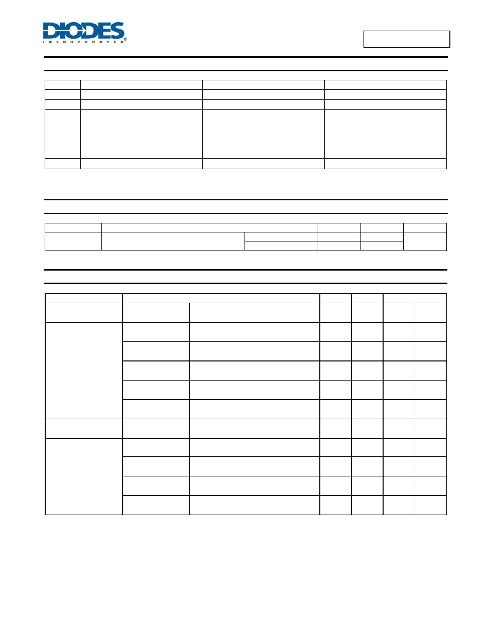
Absolute Maximum Ratings
(@T
A
= +25°C, unless otherwise specified.)
Symbol Parameter
Rating
Unit
V
IN
DC Supply Voltage
-0.3 to +18
V
T
MJ
Maximum Junction Temperature
+150
°C
P
D
Power Dissipation
SOT89-3
SOT223
TO220-3
TO252
TO263
Internally limited by maximum junction
temperature of +150°C (Note 4)
mW
T
ST
Storage Temperature
-65 to +150
°C
Notes:
4. AP1117 contains an internal thermal limiting circuit that is designed to protect the regulator in the event that the maximum junction temperature
exceeded. When activated, typically at +150°C, the regulator output switches off and then back on as the die cools
.
Recommended Operating Conditions
(@T
A
= +25°C, unless otherwise specified.)
Symbol Parameter Min
Max
Unit
T
OP
Operating Junction Temperature Range
AP1117 0
+125
°C
AP1117I -40
+125
Note: 11. 22uF is suggested for C
in
/C
out
value when application is required to work under 0
℃.
Electrical Characteristics
(@T
A
= +25°C, unless otherwise specified.)
Parameter Conditions
Min
Typ
Max
Unit
Reference Voltage
AP1117-ADJ
T
A
= +25°C, (V
IN
-
OUT
) = 1.5V
I
O
= 10mA
1.225 1.250 1.275
V
Output Voltage
AP1117-1.5
I
OUT
= 10mA, T
A
= +25°C,
3V
≤ V
IN
≤ 12V
1.470 1.500 1.530
V
AP1117-1.8
I
OUT
= 10mA, T
A
= +25°C,
3.3V
≤ V
IN
≤ 12V
1.764 1.800 1.836
V
AP1117-2.5
I
OUT
= 10mA, T
A
= +25°C,
4V
≤ V
IN
≤ 12V
2.450 2.500 2.550
V
AP1117-3.3
I
OUT
= 10mA, T
A
= +25°C,
4.8V
≤ V
IN
≤ 12V
3.235 3.300 3.365
V
AP1117-5.0
I
OUT
= 10mA, T
A
= +25°C,
6.5V
≤ V
IN
≤ 12V
4.900 5.000 5.100
V
Line Regulation
AP1117-XXX
I
O
= 10mA,V
OUT
+1.5V < V
IN
< 12V,
T
A
= 25°C
— — 0.2 %
Load Regulation
AP1117-ADJ
V
IN
= 3.3V,V
ADJ
= 0, 0mA < I
O
< 1A,
T
A
= +25°C (Notes 5, 6)
— — 1 %
AP1117-1.5
V
IN
= 3V, 0mA < I
O
< 1A,
T
A
= +25°C (Notes 5, 6)
— 12 15 mV
AP1117-1.8
V
IN
= 3.3V, 0mA < I
O
< 1A,
T
A
= +25°C (Notes 5, 6)
— 15 18 mV
AP1117-2.5
V
IN
= 4V, 0mA < I
O
< 1A,
T
A
= +25°C (Notes 5, 6)
— 20 25 mV
Notes:
5. See thermal regulation specifications for changes in output voltage due to heating effects. Line and load regulation are measured at a constant junction
temperature by low duty cycle pulse testing. Load regulation is measured at the output lead = 1/18” from the package.
6. Line and load regulation are guaranteed up to the maximum power dissipation of 15W. Power dissipation is determined by the difference between input
and output differential and the output current. Guaranteed maximum power dissipation will not be available over the full input/output range.