Electrical characteristics, Ap1115 – Diodes AP1115 User Manual
Page 4
AP1115
Document number: DS31025 Rev. 11 - 2
4 of 8
August 2012
© Diodes Incorporated
AP1115
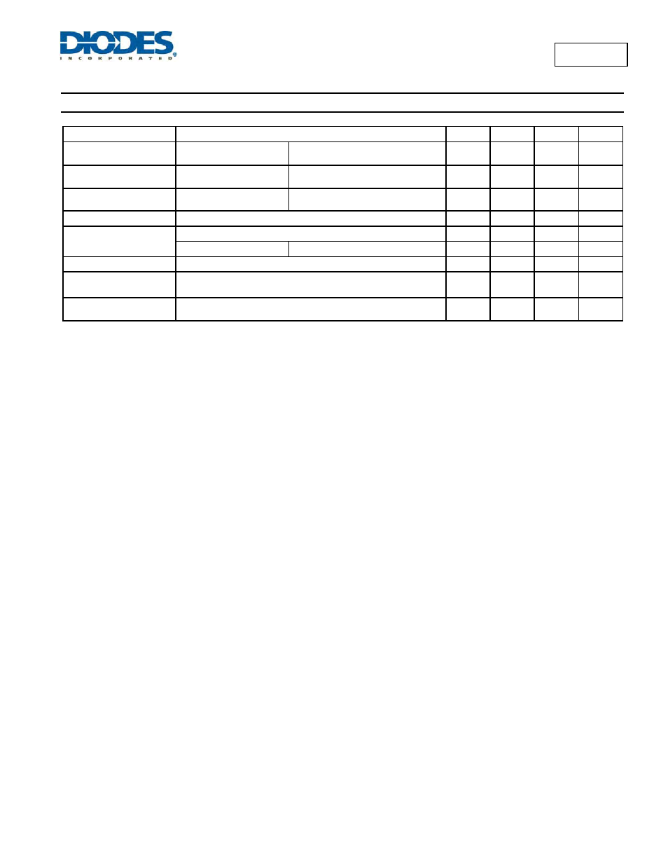
Electrical Characteristics
(cont.)
(@T
A
= +25°C, unless otherwise specified.)
Parameter Conditions
Min
Typ
Max
Unit
Dropout Voltage (V
IN
-V
OUT
)
AP1115-ADJ/1.5/1.8
2.5/2.8/3.0/3.3/3.5/5.0
I
OUT
= 0.6A,
ΔV
OUT
= 1%V
OUT
—
1.1 1.3 V
Current Limit
AP1115-ADJ/1.5/1.8
2.5/2.8/3.0/3.3/3.5/5.0
(V
IN
-V
OUT
) = 5V
0.7
—
—
A
Minimum Load Current
(Note 6)
AP1115-XXX 0°C
≤ T
J
≤ +125°C
—
5
10
mA
Thermal Regulation
T
A
= +25°C, 30ms pulse
—
0.008
0.04
%/W
Ripple Rejection
f = 120Hz,C
OUT
= 25µF Tantalum, I
OUT
=
0.6A
AP1115-XXX V
IN
= V
OUT
+3V —
60
70
dB
Temperature Stability
I
O
= 10mA
—
0.6
—
%
θ
JA
Thermal Resistance Junction-to-Ambient
(No heat sink; No air flow) (Note 7)
— 164 —
°C/W
θ
JC
Thermal Resistance Junction-to-Case
Control Circuitry/Power Transistor (Note 7)
— 35 —
°C/W
Notes:
6. Quiescent current is defined as the minimum output current required to maintain regulation. At 12V input/output differential the device is guaranteed to
regulate if the output current is greater than 10mA.
7. Test conditions for SOT89-3L: Device mounted on FR-4 substrate, 2oz copper, with minimum recommended pad layout.