Ap1115, Typical applications circuit, Pin descriptions – Diodes AP1115 User Manual
Page 2
AP1115
Document number: DS31025 Rev. 11 - 2
2 of 8
August 2012
© Diodes Incorporated
AP1115
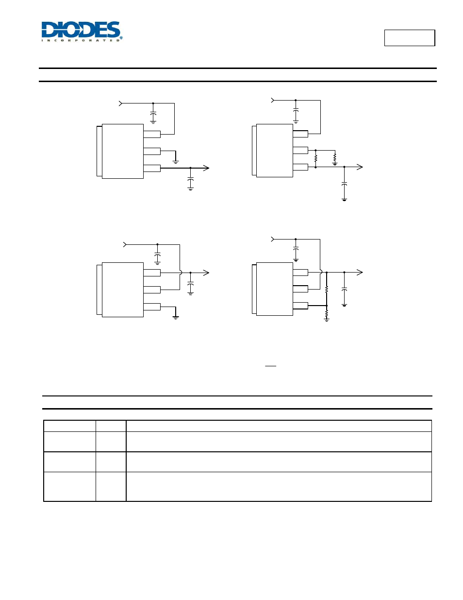
Typical Applications Circuit
C2
100uF
5V
3.3V/0.5A
V
IN
V
OUT
GND
C1
100uF
AP1115 A (5V/3.3V Fixed Output)
)
1
2
REF
o
R
R
(1
V
V
Note :
GND
AP1115 B (5V/3.3V Fixed Output)
5V
C1
100uF
C2
100uF
3.3V/0.5A
R1
121
R2
121
C2
100uF
5V
2.5V/0.5A
Adj
C1
100uF
V
O
AP1115 A (5V/2.5V Adj Output)
R2
121
R1
121
C2
100 uF
5V
2.5V/0.5A
Adj
C1
100uF
V
O
AP1115 B (5V/2.5V Adj Output)
Ω
Ω
Ω
Ω
=
+
V
IN
V
OUT
V
OUT
V
IN
V
OUT
V
IN
x
Pin Descriptions
Pin Name
I/O
Function
Adj (GND)
I
A resistor divider from this pin to the V
OUT
pin and ground sets the output voltage (Ground only for Fixed-
Mode).
V
OUT
O
The output of the regulator. A minimum of 10uF capacitor (0.15
Ω ≤ ESR ≤ 20Ω) must be connected from this
pin to ground to insure stability.
V
IN
I
The input pin of regulator. Typically a large storage capacitor (0.15
Ω ≤ ESR ≤ 20Ω) is connected from this pin
to ground to insure that the input voltage does not sag below the minimum dropout voltage during the load
transient response. This pin must always be 1.3V higher than V
OUT
in order for the device to regulate properly.