Absolute maximum ratings, Recommended operating conditions, Electrical characteristics – Diodes AP1115 User Manual
Page 3: Ap1115
AP1115
Document number: DS31025 Rev. 11 - 2
3 of 8
August 2012
© Diodes Incorporated
AP1115
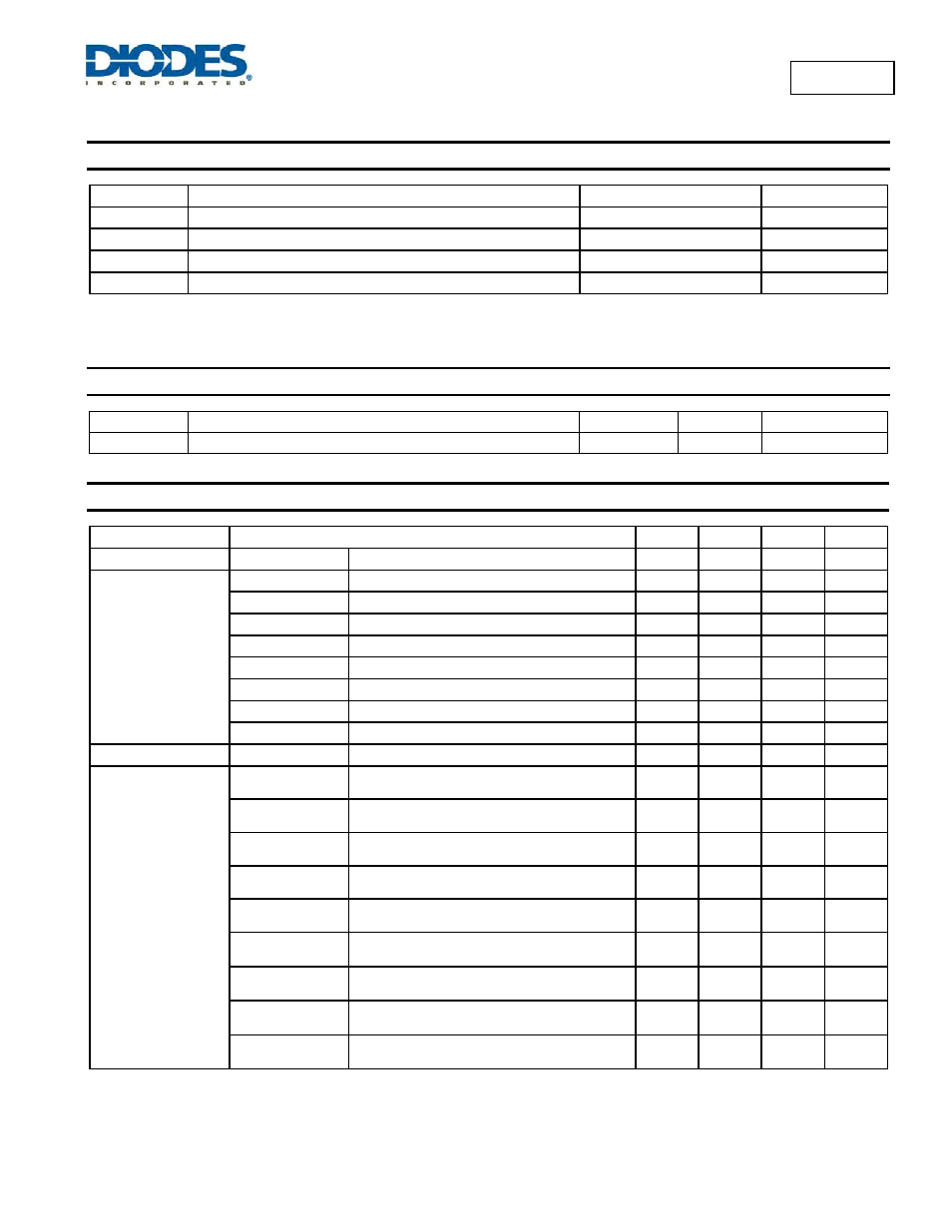
Absolute Maximum Ratings
(@T
A
= +25°C, unless otherwise specified.)
Symbol Parameter
Rating
Unit
V
IN
DC Supply Voltage
-0.3 to +18
V
P
D
Power Dissipation
Internally Limited
mW
T
ST
Storage Temperature
-65 to +150
°C
T
MJ
Maximum Junction Temperature
+150
°C
Stresses greater than the 'Absolute Maximum Ratings' specified above, may cause permanent damage to the device. These are stress ratings only; functional
operation of the device at these or any other conditions exceeding those indicated in this specification is not implied. Device reliability may be affected by exposure to
absolute maximum rating conditions for extended periods of time.
Recommended Operating Conditions
Symbol Parameter
Min
Max
Unit
T
OP
Operating Junction Temperature Range
0
+125
°C
Electrical Characteristics
(@T
A
= +25°C, unless otherwise specified.)
Parameter Conditions
Min
Typ
Max
Unit
Reference Voltage
AP1115-ADJ
T
A
= +25°C, (V
IN
-
OUT
) = 1.5V, I
O
= 10mA
1.225 1.250 1.275
V
Output Voltage
AP1115-1.5
I
OUT
= 10mA, T
A
= +25°C, 3V
≤ V
IN
≤ 12V
1.470 1.500 1.530
V
AP1115-1.8
I
OUT
= 10mA, T
A
= +25°C, 3.3V
≤ V
IN
≤ 12V
1.764 1.800 1.836
V
AP1115-2.5
I
OUT
= 10mA, T
A
= +25°C, 4V
≤ V
IN
≤ 12V
2.450 2.500 2.550
V
AP1115-2.8
I
OUT
= 10mA, T
A
= +25°C, 4.3V
≤ V
IN
≤ 12V
2.744 2.800 2.856
V
AP1115-3.0
I
OUT
= 10mA, T
A
= +25°C, 4.5V
≤ V
IN
≤ 12V
2.940 3.000 3.060
V
AP1115-3.3
I
OUT
= 10mA, T
A
= +25°C, 4.8V
≤ V
IN
≤ 12V
3.235 3.300 3.365
V
AP1115-3.5
I
OUT
= 10mA, T
A
= +25°C, 5V
≤ V
IN
≤ 12V
3.430 3.500 3.570
V
AP1115-5.0
I
OUT
= 10mA, T
A
= +25°C, 6.5V
≤ V
IN
≤ 12V
4.900 5.000 5.100
V
Line Regulation
AP1115-XXX
I
O
= 10mA, V
OUT
+ 1.5V < V
IN
< 15V, T
A
= +25°C
— — 0.2 %
Load Regulation
AP1115-ADJ
V
IN
= 3.3V, V
ADJ
= 0,0mA < Io < 0.6A,
T
A
= +25°C (Notes 4 & 5)
— — 1 %
AP1115-1.5
V
IN
= 3V, 0mA < Io < 0.6A,T
A
= +25°C
(Notes 4 & 5)
— 12 15 mV
AP1115-1.8
V
IN
= 3.3V, 0mA < Io < 0.6A, T
A
= +25°C
(Notes 4 & 5)
— 15 18 mV
AP1115-2.5
V
IN
= 4V, 0mA < Io < 0.6A, T
A
= +25°C
(Notes 4 & 5)
— 20 25 mV
AP1115-2.8
V
IN
= 4.3V, 0mA < Io < 0.6A, T
A
= +25°C
(Notes 4 & 5)
— 22 28 mV
AP1115-3.0
V
IN
= 5V, 0
≤ I
OUT
≤ 0.6A, T
A
= +25°C
(Notes 4 & 5)
— 23 30 mV
AP1115-3.3
V
IN
= 5V, 0
≤ I
OUT
≤ 0.6A, T
A
= +25°C
(Notes 4 & 5)
— 26 33 mV
AP1115-3.5
V
IN
= 5V, 0
≤ I
OU
T
≤ 0.6A, T
A
= +25°C
(Notes 4 & 5)
— 28 35 mV
AP1115-5.0
V
IN
= 8V, 0
≤ I
OU
T
≤ 0.6A, T
A
= +25°C
(Notes 4 & 5)
— 40 50 mV
Notes:
4. See thermal regulation specifications for changes in output voltage due to heating effects. Line and load regulation are measured at a constant
junction temperature by low duty cycle pulse testing. Load regulation is measured at the output lead = 1/18” from the package.
5. Line and load regulation are guaranteed up to the maximum power dissipation of 5W. Power dissipation is determined by the input/output differential
and the output current. Guaranteed maximum power dissipation will not be available over the full input/output range.