Absolute maximum ratings, Dissipation rating table, Recommended operating conditions – Diodes AP2552/ AP2553/ AP2552A/ AP2553A User Manual
Page 4

AP2552/AP2553/AP2552A/AP2553A
Document number: DS35404 Rev. 8 - 2
4 of 16
February 2014
© Diodes Incorporated
AP2552/ AP2553/ AP2552A/ AP2553A
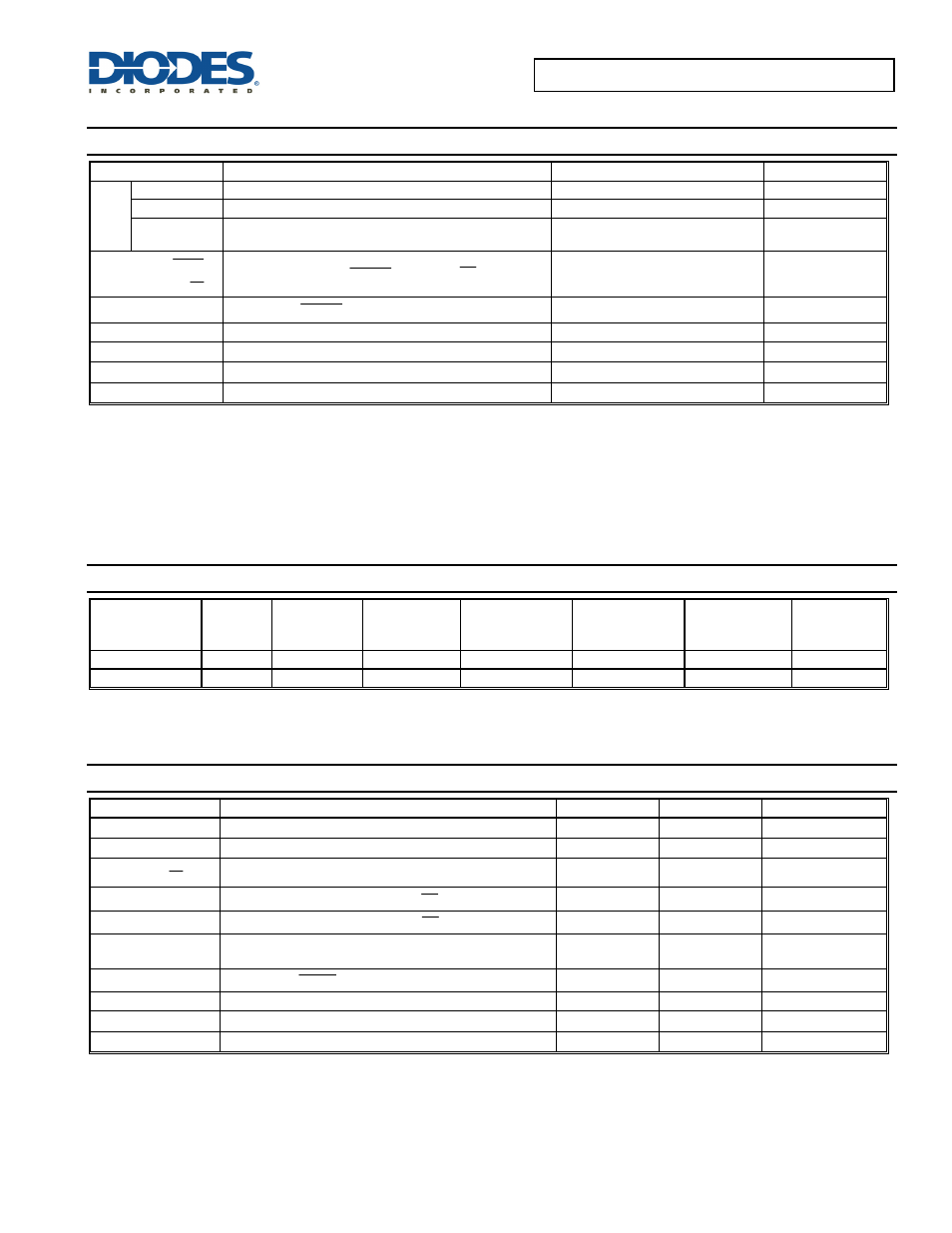
Absolute Maximum Ratings
(@T
A
= +25°C, unless otherwise specified.)
Symbol Parameter
Ratings
Unit
ESD
HBM
Human Body Model ESD Protection
2
kV
CDM
Charged Device Model ESD Protection
500
V
IEC system
level
Surges per EN61000-4-2. 1999 applied to output
terminals of EVM Note (5)
15 kV
V
IN
, V
OUT
, V
FAULT
,
VILIM,
,
EN
V
EN
V
Voltage on IN, OUT,
FAULT
, ILIM, EN,
EN
-0.3 to +6.5
V
—
Continuous
FAULT
sink current
25 mA
— ILIM
source
current
1
mA
I
LOAD
Maximum Continuous Load Current
Internal Limited
A
T
J(MAX)
Maximum Junction Temperature
-40 to +150
°C
T
ST
Storage Temperature Range (Note 4)
-65 to +150
°C
Notes: 4. UL Recognized Rating from -30°C to +70°C (Diodes qualified T
ST
from -65°C to +150°C)
5. External capacitors need to be connected to the output, EVM board was tested with capacitor 2.2uF 50V 0805. This level is a pass test only and not a
limit.
Caution: Stresses greater than the 'Absolute Maximum Ratings' specified above, may cause permanent damage to the device. These are stress ratings only;
functional operation of the device at these or any other conditions exceeding those indicated in this specification is not implied. Device reliability may be
affected by exposure to absolute maximum rating conditions for extended periods of time.
Semiconductor devices are ESD sensitive and may be damaged by exposure to ESD events. Suitable ESD precautions should be taken when
handling and transporting these devices.
Dissipation Rating Table
Board Package
Thermal
Resistance
θ
JA
Thermal
Resistance
θ
JC
T
A
≤ +25°C
Power
Rating
Derating Factor
Above
T
A
= +25°C
T
A
= +70°C
Power Rating
T
A
= +85°C
Power
Rating
High-K (Note 6)
W6
160°C/W 55°C/W 625mW 6.25mW/°C 340mW 250mW
High-K (Note 6)
FDC
120°C/W 34°C/W 833mW 8.33mW/°C 450mW 330mW
Note:
6. The JEDEC high-K (2s2p) board used to derive this data was a 3in x 3in, multilayer board with 1-ounce internal power and ground planes with
2-ounce copper traces on top and bottom of the board.
Recommended Operating Conditions
(@T
A
= +25°C, unless otherwise specified.)
Symbol Parameter Min
Max
Unit
V
IN
Input Voltage
2.7
5.5
V
I
OUT
Continuous Output Current (-40°C ≤ T
A
≤ +85°C)
0 2.1 A
,
EN
V
EN
V
Enable Voltage
0
5.5
V
V
IH
High-Level Input Voltage on EN or EN
2.0
V
IN
V
V
IL
Low-Level Input Voltage on EN or EN
0 0.8 V
R
LIM
Current-Limit Threshold Resistor Range
(1% initial tolerance)
10 210 kΩ
I
O
Continuous
FAULT
Sink Current
0 10 mA
Input De-Coupling Capacitance, IN to GND
0.1
µF
T
A
Operating Ambient Temperature
-40
+85
C
T
J
Operating Junction Temperature
-40
+125
C
