Typical applications circuit, Available options, Pin descriptions – Diodes AP2552/ AP2553/ AP2552A/ AP2553A User Manual
Page 2
AP2552/AP2553/AP2552A/AP2553A
Document number: DS35404 Rev. 8 - 2
2 of 16
February 2014
© Diodes Incorporated
AP2552/ AP2553/ AP2552A/ AP2553A
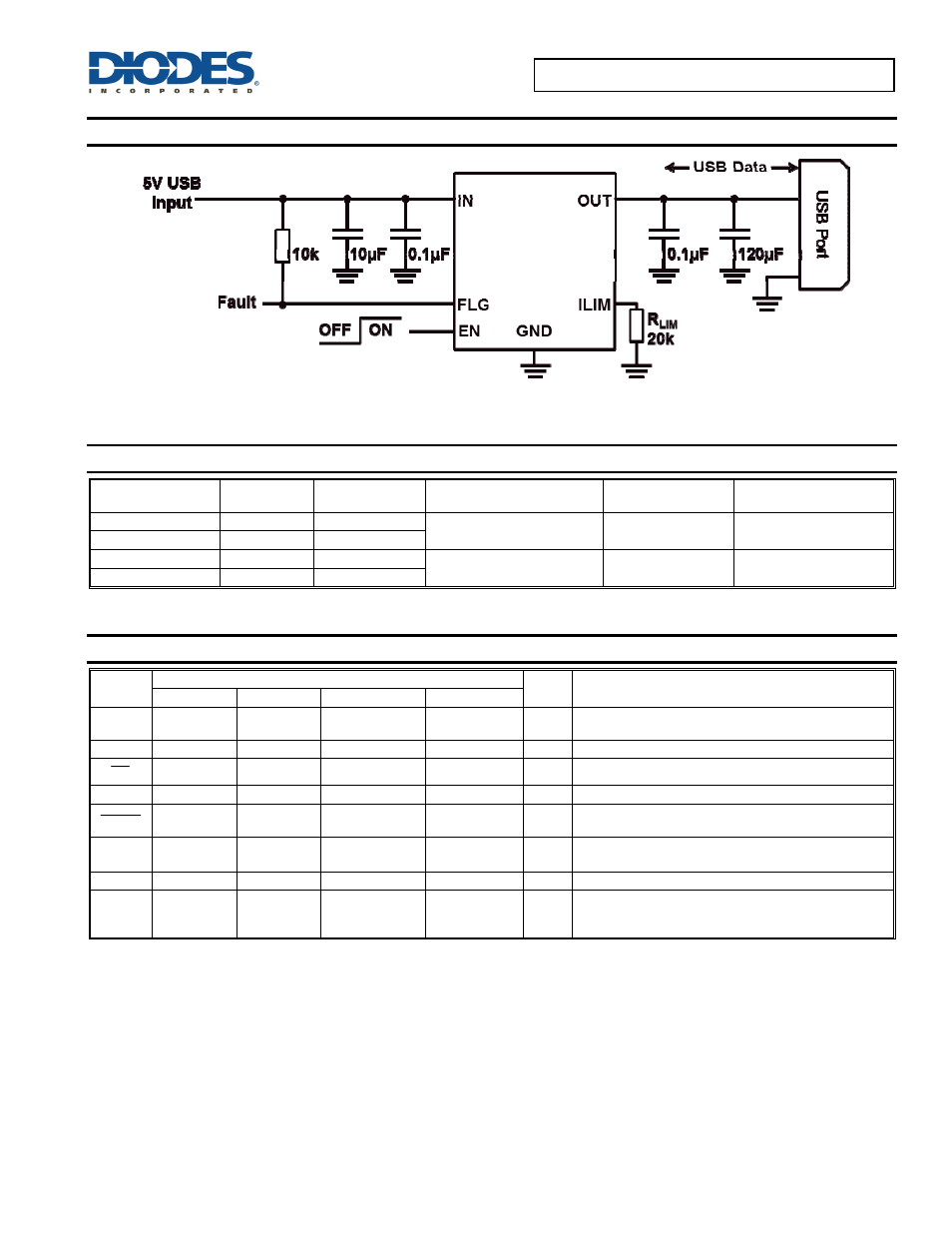
Typical Applications Circuit
120µF Output Capacitance is a Requirement of USB
Available Options
Part Number
Channel
Enable Pin (EN)
Recommended Maximum
Continuous Load Current (A)
Current-Limit
Protection
Package
AP2552 1
Active
Low
2.1 Constant-Current
U-DFN2020-6
SOT26
AP2553 1
Active
High
AP2552A 1
Active
Low
2.1 Latch-Off
U-DFN2020-6
SOT26
AP2553A 1
Active
High
Pin Descriptions
Pin
Name
Pin Number
I/O Function
AP2552W6-7 AP2553W6-7 AP2552FDC-7 AP2553FDC-7
IN 1 1
6
6 I
Input, connect a 0.1µF or greater ceramic capacitor from
IN to GND as close to IC as possible.
GND
2
2
5
5
—
Ground, connect to external exposed pad.
EN
3
—
4
—
I
Enable input, logic low turns on power switch.
EN
—
3
—
4
I
Enable input, logic high turns on power switch.
FAULT
4 4 3
3
O
Active-low open-drain output, asserted during over-
current, over-temperature, or reverse-voltage conditions.
ILIM 5
5
2
2 O
Use external resistor to set current-limit threshold;
recommended 10kΩ≦RLIM≦232kΩ.
OUT 6
6
1
1 O
Output
Exposed
Pad
— — Pad Pad
—
No internal connection; recommend to connect to GND
externally for improved power dissipation. . It should not
be used as electrical ground conduction path.