Ap3417c preliminary datasheet, Functional block diagram, Absolute maximum ratings – Diodes AP3417C User Manual
Page 3
AP3417C
Document number: DS36516 Rev. 1 - 0
3 of 11
www.diodes.com
September 2013
© Diodes Incorporated
AP3417C
PRELIMINARY DATASHEET
A Product Line of
Diodes Incorporated
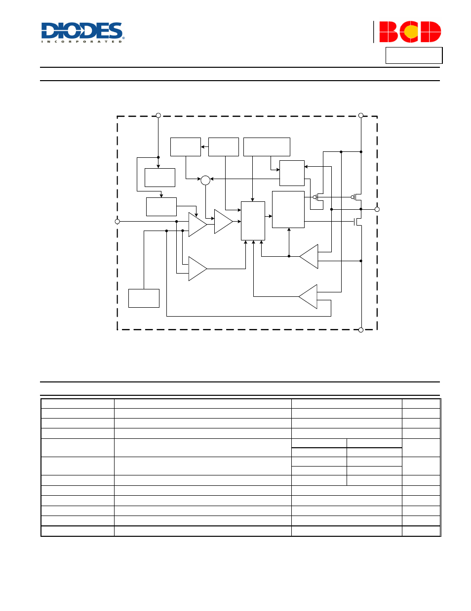
Functional Block Diagram
Over - Current
Comparator
Bias
Generator
Saw-tooth
Generator
Oscillator
Soft
Start
Bandgap
Reference
Current
Sensing
Control
Logic
Buffer &
Dead Time
Control
Logic
+
Reverse Inductor
Current Comparator
Over Voltage
Comparator
Modulator
Error
Amplifier
-
+
-
+
-
+
-
+
GND
EN
FB
LX
1(2)
VIN
4(3)
3(4)
2(5)
5(6)
A(B)
A for SOT-23-5
B for DFN-2×2-6
-
+
IOVP Comparator
Absolute Maximum Ratings
(Note 1)
Symbol Parameter
Rating
Unit
V
IN
Input Voltage for the MOSFET Switch
0 to 6.0
V
V
EN
Enable Input Voltage
-0.3 to V
IN
+0.3
V
I
LX
LX Pin Switch Current
1.8
A
P
D
Power Dissipation (On PCB, T
A
= +25°C)
SOT-23-5 0.4
W
DFN-2×2-6 1.89
θ
JA
Thermal Resistance (Junction to Ambient, Simulation)
SOT-23-5 250
°C/W
DFN-2×2-6 53
θ
JC
Thermal Resistance (Junction to Case, Simulation)
SOT-23-5
130
°C/W
T
J
Operating Junction Temperature
155
°C
T
STG
Storage Temperature
-55 to +150
°C
T
OP
Operating Temperature
-40 to +85
°C
V
MM
ESD (Machine Model)
200
V
V
HBM
ESD (Human Body Model)
2000
V
Note:
1. Stresses greater than those listed under “Absolute Maximum Ratings” may cause permanent damage to the device. These are stress ratings only, and
functional operation of the device at these or any other conditions beyond those indicated under “Recommended Operating Conditions” is not implied.
Exposure to “Absolute Maximum Ratings” for extended periods may affect device reliability.