Application information, Al5801 – Diodes AL5801 User Manual
Page 7
AL5801
Document number: DS35555 Rev. 3 - 2
7 of 11
July 2012
© Diodes Incorporated
AL5801
Application Information
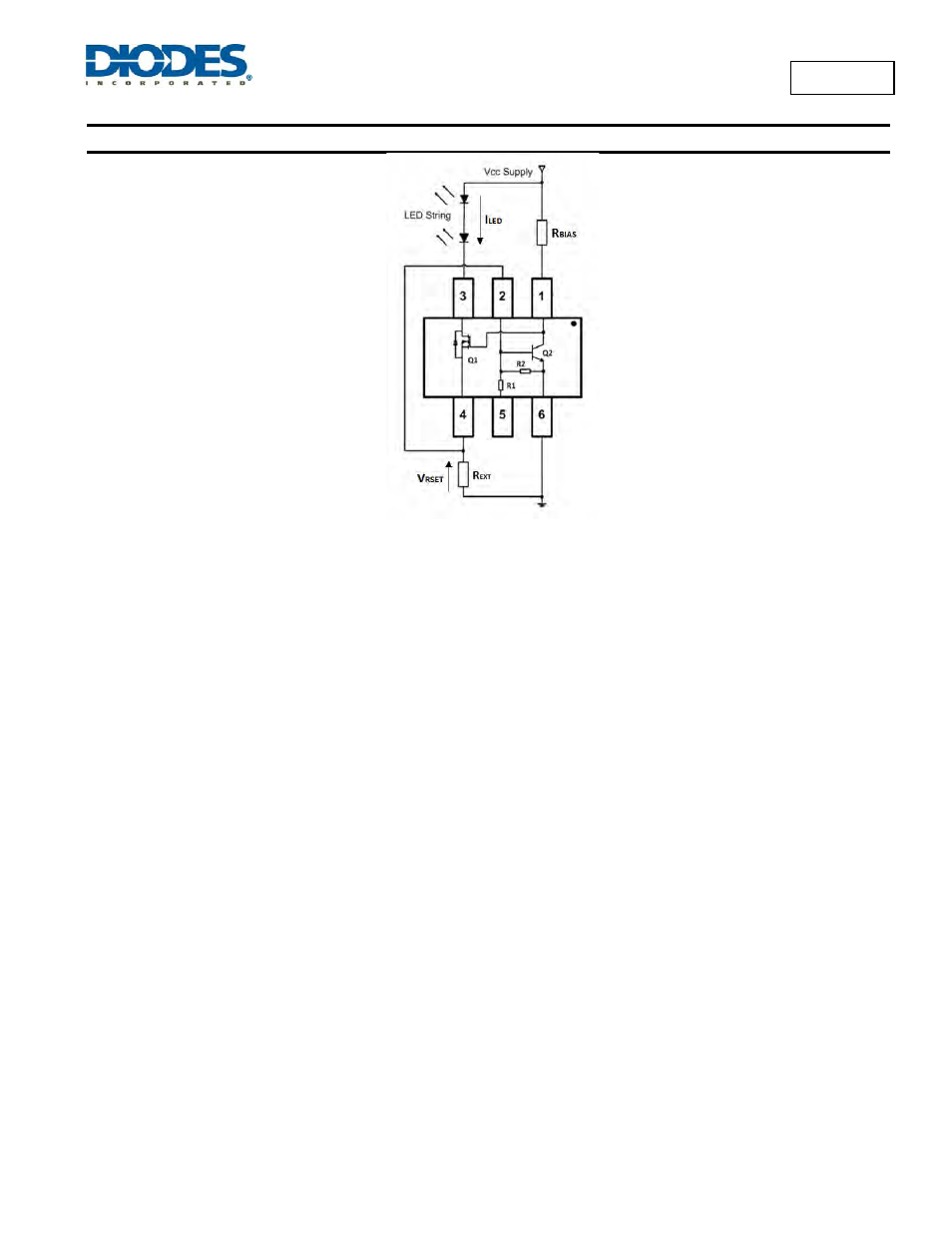
Figure 13 Typical Application Circuit for
Linear Mode Current Sink LED Driver
The AL5801 is designed for driving high brightness LEDs with typical LED current up to 350mA. It provides a more cost effective way for driving
low current LEDs when compared against more complex switching regulator solutions. Furthermore, it reduces the PCB board area of the
solution because there is no need for external components like inductors, capacitors and/or switching diodes.
Figure 13 shows a typical application circuit diagram for driving an LED or a string of LEDs. The NPN transistor Q2 measures the LED current by
sensing the voltage across an external resistor R
EXT
. Q2 uses its V
BE
as reference to set the voltage across R
EXT
and controls the gate voltage of
MOSFET Q1. Q1 operates in linear mode to regulate the LED current. The LED current is:
I
LED
= V
RSET
/ R
EXT
where V
RSET
is the V
BE
of Q2. V
BE
is 0.56V typical at a +25°C device temperature. See Figure 11 for the variation of V
BE
with Q2’s junction
temperature at I
BIAS
= 0.1mA. V
BE
has a negative temperature coefficient which reduces the LED current as the device warms up, protecting the
LED(s).
R
BIAS
should be chosen to drive 0.1mA current into the BIAS pin
R
BIAS
= ( V
CC
– 3.75V ) / 0.1mA
From the above equation, for any required LED current the necessary external resistor R
EXT
can be calculated from
R
EXT
= V
RSET
/ I
LED
The expected linear mode power dissipation must be factored into the design consideration. The power dissipation across the device can be
calculated by taking the maximum supply voltage less the minimum voltage across the LED string.
V
DS(Q1)
= V
CC(max)
– V
LED(min)
– V
RSET
P
D
= V
DS(Q1)
* I
LED
As the output LED current of AL5801 increases so will its power dissipation. The power dissipation will cause the device temperature to rise
above ambient,
T
A
, by an amount determined by the package thermal resistance, R
θJA
.
Therefore, the power dissipation supported by the device is dependent upon the PCB board material, the copper area and the ambient
temperature. The maximum dissipation the device can handle is given by:
P
D
= ( T
J(MAX)
- T
A
) / R
θJA
T
J(MAX)
= +
150°C
is the maximum device junction temperature. Refer to the thermal characteristic graphs in Figure 2 to 4 for selecting the
appropriate PCB copper area. Figure 12 shows the current capabilities of the AL5801 at +
25°C
with different PCB copper area heat sinks.