Al5801, Pin descriptions, Functional block diagram – Diodes AL5801 User Manual
Page 2: Absolute maximum ratings
AL5801
Document number: DS35555 Rev. 3 - 2
2 of 11
July 2012
© Diodes Incorporated
AL5801
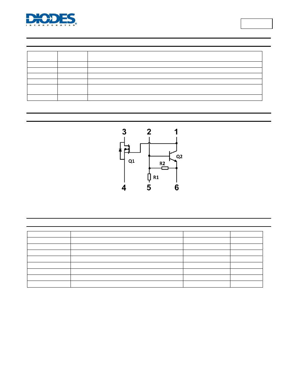
Pin Descriptions
Pin
Number
Pin
Name
Function
1
BIAS
Biases the open-Drain output MOSFET
2 FB
Feedback
pin
3
OUT
Open-Drain LED driver output
4 R
EXT
Current sense pin. LED current sensing resistor should be connected from here to GND
5 COMP
Compensation pin. Connect COMP pin to REXT pin and insert a 1nF ceramic capacitor from COMP
pin to FB pin for improved transient stability
6
GND
Ground reference point for setting the LED current
Functional Block Diagram
Figure 1 Block Diagram
Absolute Maximum Ratings
(@T
A
= +25°C, unless otherwise specified.)
Symbol Characteristics Values
Unit
V
OUT
Output voltage relative to GND
100
V
V
BIAS
BIAS voltage relative to GND (Note 4)
20
V
V
FB
FB voltage relative to GND
6
V
V
COMP
COMP voltage relative to GND
6
V
V
REXT
REXT voltage relative to GND
6
V
I
OUT
Output current
350
mA
T
J
Operating junction temperature
-40 to +150
°C
T
ST
Storage temperature
-55 to +150
°C
Note:
4. With pins 5 and 6 connected together.
These are stress ratings only. Operation outside the absolute maximum ratings may cause device failure.
Operation at the absolute maximum rating for extended periods may reduce device reliability.