Al5801, Package thermal data, Recommended operating conditions – Diodes AL5801 User Manual
Page 3: Nmosfet electrical characteristics: (q1)
AL5801
Document number: DS35555 Rev. 3 - 2
3 of 11
July 2012
© Diodes Incorporated
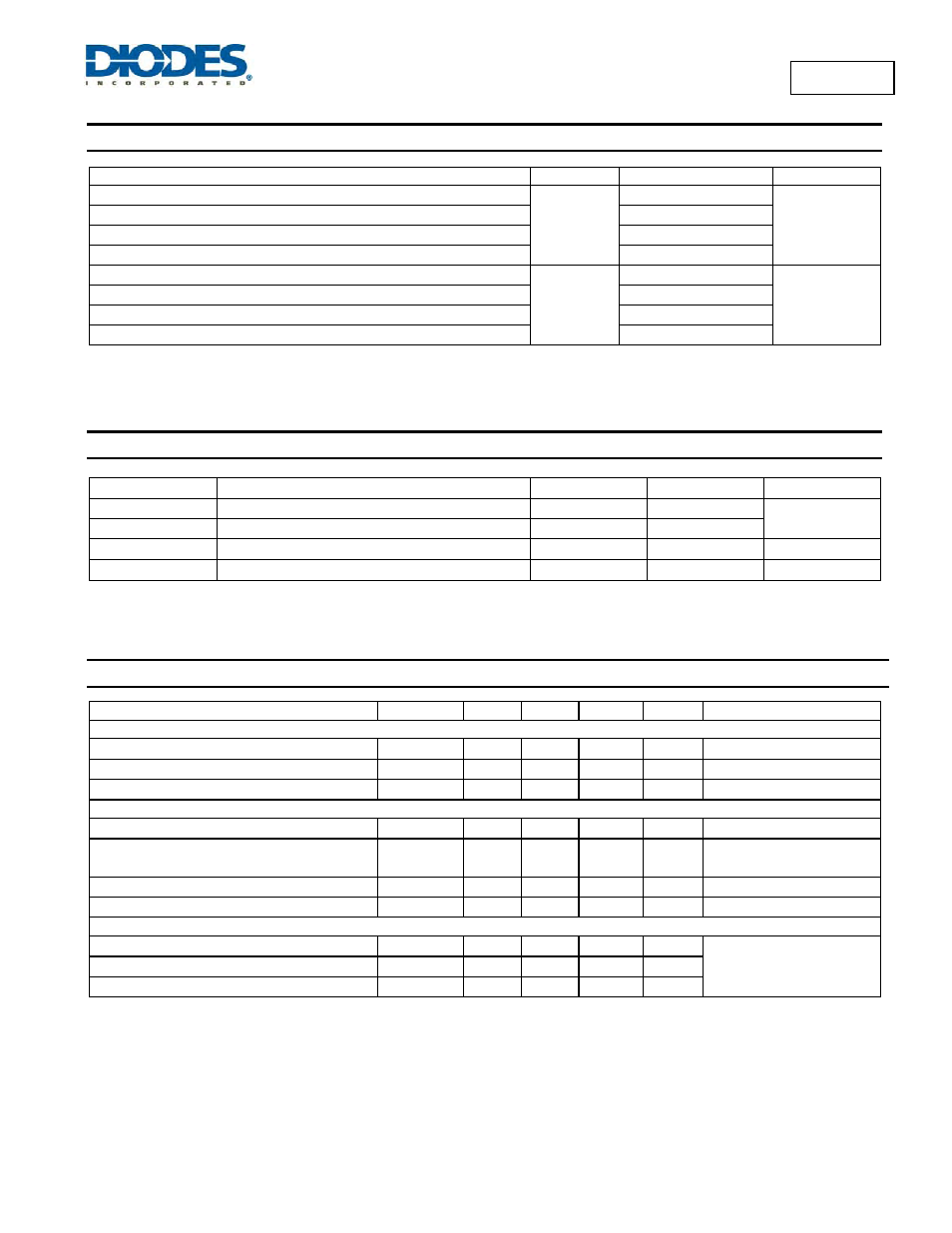
AL5801
Package Thermal Data
Characteristic Symbol
Value
Unit
Power Dissipation (Note 5) @ T
A
= +25°C
P
D
0.75
W
Power Dissipation (Note 6) @ T
A
= +25°C
0.70
Power Dissipation (Note 7) @ T
A
= +25°C
0.85
Power Dissipation (Note 8) @ T
A
= +25°C
1.05
Thermal Resistance, Junction to Ambient Air (Note 5) @ T
A
= +25°C
R
θJA
165
°C/W
Thermal Resistance, Junction to Ambient Air (Note 6) @ T
A
= +25°C
180
Thermal Resistance, Junction to Ambient Air (Note 7) @ T
A
= +25°C
145
Thermal Resistance, Junction to Ambient Air (Note 8) @ T
A
= +25°C
120
Notes:
5. Device mounted on 15mm x 15mm 2oz copper board.
6. Device mounted on 25mm x 25mm 1oz copper board.
7. Device mounted on 25mm x 25mm 2oz copper board.
8. Device mounted on 50mm x 50mm 2oz copper board.
Recommended Operating Conditions
(@T
A
= +25°C, unless otherwise specified.)
Symbol Parameter Min
Max
Unit
V
BIAS
Supply voltage range
3.5
20
V
V
OUT
OUT voltage range
1.1
100
I
LED
LED pin current (Note 9)
25
350
mA
T
A
Operating ambient temperature range
-40
125
°C
Note:
9. Subject to ambient temperature, power dissipation and PCB.
NMOSFET Electrical Characteristics: (Q1)
(@T
A
= +25°C, unless otherwise specified.)
Characteristic
Symbol Min Typ Max Unit
Test
Condition
OFF CHARACTERISTICS
Drain-Source Breakdown Voltage
BV
DSS
100
⎯
⎯
V
V
GS
= 0V, I
D
= 250µA
Zero Gate Voltage Drain Current
I
DSS
⎯
⎯
1 µA
V
DS
= 60V, V
GS
= 0V
Gate-Source Leakage
I
GSS
⎯
⎯
±100
nA
V
GS
=
±20V, V
DS
= 0V
ON CHARACTERISTICS
Gate Threshold Voltage
V
GS(th)
2.0
⎯
4.1 V
V
DS
= V
GS
, I
D
= 250µA
Static Drain-Source On-Resistance
R
DS (ON)
⎯
⎯
⎯
0.85
0.99
Ω
V
GS
= 10V, I
D
= 1.5A
V
GS
= 6V, I
D
= 1A
Forward Transconductance
g
fs
⎯
0.9
⎯
S
V
DS
= 15V, I
D
= 1A
Diode Forward Voltage
V
SD
⎯
0.89 1.1 V
V
GS
= 0V, I
S
= 1.5A
DYNAMIC CHARACTERISTICS
Input Capacitance
C
iss
⎯
129
⎯
pF
V
DS
= 50V, V
GS
= 0V
f = 1.0MHz
Output Capacitance
C
oss
⎯
14
⎯
pF
Reverse Transfer Capacitance
C
rss
⎯
8
⎯
pF