Zxld1360, Application information – Diodes ZXLD1360 User Manual
Page 20
ZXLD1360
ZXLD1360
Document number: DS33471 Rev. 4 - 2
20 of 25
March 2011
© Diodes Incorporated
A Product Line of
Diodes Incorporated
Application Information
(cont.)
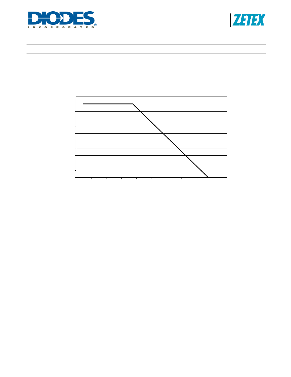
Thermal considerations
When operating the device at high ambient temperatures, or when driving maximum load current, care must be taken to
avoid exceeding the package power dissipation limits. The graph below gives details for power derating. This assumes the
device to be mounted on a 25mm x 25mm PCB with 1oz copper standing in still air.
Note that the device power dissipation will most often be a maximum at minimum supply voltage. It will also increase if the
efficiency of the circuit is low. This may result from the use of unsuitable coils, or excessive parasitic output capacitance on
the switch output.
Thermal compensation of output current
High luminance LEDs often need to be supplied with a temperature compensated current in order to maintain stable and
reliable operation at all drive levels. The LEDs are usually mounted remotely from the device so, for this reason, the
temperature coefficients of the internal circuits for the ZXLD1360 have been optimized to minimize the change in output
current when no compensation is employed. If output current compensation is required, it is possible to use an external
temperature sensing network - normally using Negative Temperature Coefficient (NTC) thermistors and/or diodes, mounted
very close to the LED(s). The output of the sensing network can be used to drive the ADJ pin in order to reduce output
current with increasing temperature.
Maximum Power Dissipation
0
100
200
300
400
500
600
700
800
900
1000
1100
-50
-30
-10
10
30
50
70
90
110
130
150
Ambient Temperature (Deg C)
Po
we
r
(m
W)