Zxld1360, Application information – Diodes ZXLD1360 User Manual
Page 13
ZXLD1360
ZXLD1360
Document number: DS33471 Rev. 4 - 2
13 of 25
March 2011
© Diodes Incorporated
A Product Line of
Diodes Incorporated
Application Information
Setting nominal average output current with external resistor R
S
The nominal average output current in the LED(s) is determined by the value of the external current sense resistor (R
S
)
connected between V
IN
and I
SENSE
and is given by:
I
OUTnom
= 0.1/R
S
[for R
S
> 0.1Ω]
The table below gives values of nominal average output current for several preferred values of current setting resistor (R
S
) in
the typical application circuit shown on page 1:
R
S
(
Ω)
Nominal average
output current (mA)
0.1 1000
0.13 760
0.15 667
The above values assume that the ADJ pin is floating and at a nominal voltage of V
REF
(=1.25V). Note that R
S
= 0.1V is the
minimum allowed value of sense resistor under these conditions to maintain switch current below the specified maximum
value.
It is possible to use different values of R
S
if the ADJ pin is driven from an external voltage. (See next section).
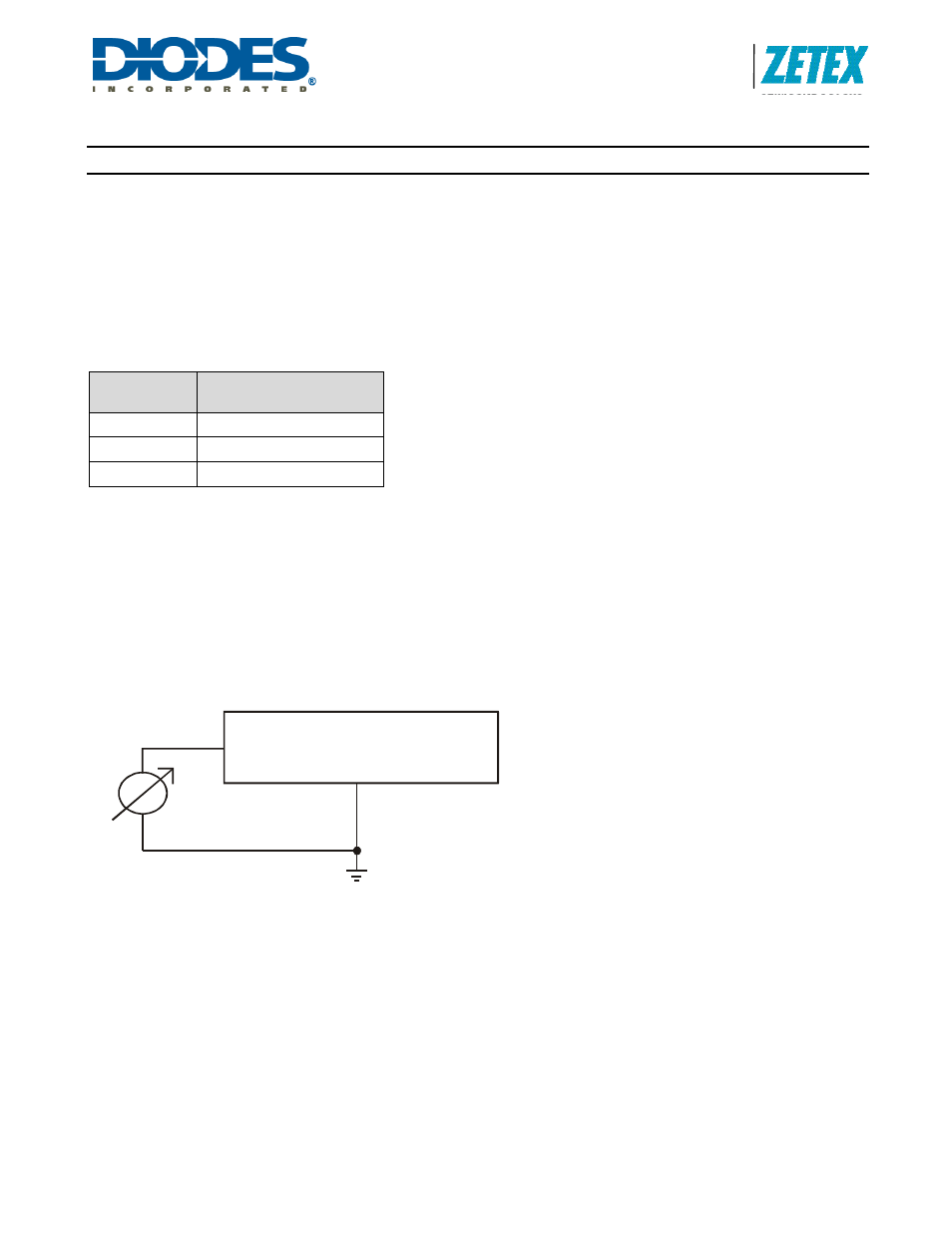
Output current adjustment by external DC control voltage
The ADJ pin can be driven by an external dc voltage (V
ADJ
), as shown, to adjust the output current to a value above or below
the nominal average value defined by R
S
.
The nominal average output current in this case is given by:
I
OUTdc
= (V
ADJ
/1.25) x (100mV/R
S
) [for 0.3< V
ADJ
<2.5V]
Note that 100% brightness setting corresponds to V
ADJ
= V
REF
. When driving the ADJ pin above 1.25V, R
S
must be
increased in proportion to prevent I
OUTdc
exceeding 550mA maximum.
The input impedance of the ADJ pin is 50k
Ω ±25% for voltages below V
REF
and 20k
Ω ±25% for voltages above V
REF
+100mV.
G ND
ZXLD1360
ADJ
GND
+
DC