Iii. installation, Layout of the asus p2b98-xv motherboard, Board layout iii. inst alla tion – Asus P2B98-XV User Manual
Page 10
10
ASUS P2B98-XV User’s Manual
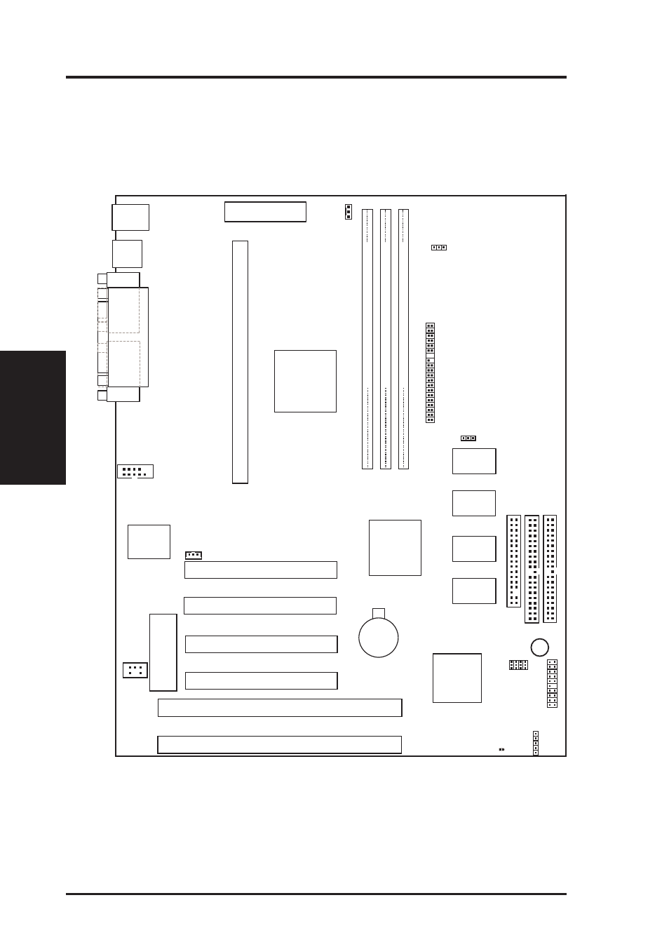
III. INSTALLATION
Layout of the ASUS P2B98-XV Motherboard
USB
PS/2
VGA
COM 1
FSB
BF0
BF1
BF2
BF3
0 1
2 3
4 5
SYS_FAN
COM2
CLRTC
CPU_FAN
Floppy Disk Drive
INT_EN
2 MB SDRAM
2 MB SDRAM
2 MB SDRAM
2 MB SDRAM
Wake-On-LAN
Connector
Intel
440BX
AGPset
DIMM Socket 2 (64-bit, 168-pin module)
DIMM Socket 3 (64-bit, 168-pin module)
Single Edge Contact Slot
DIMM Socket 1 (64-bit, 168-pin module)
USB 1(TOP PORT)
USB 2 (BOTTOM)
MOUSE (TOP PORT)
KEYBOARD (BOTTOM)
P
ARALLEL
PORT
Keyboard
BIOS &
Multi-I/O
Chip
Flash EEPROM
(Programable BIOS)
PCI Slot 1
PCI Slot 2
PCI Slot 3
PCI Slot 4
ISA Slot 1
ISA Slot 2
Onboard
ATI AGP 2X
VGA
Chipset
Intel PIIX4E
PCIset
CMOS Power
(CR2032 3V
Lithium Cell)
Secondary IDE
Primary IDE
ATX Power Connector
AMC Connector
BUS Freq.
Row
Panel Connectors
Buzzer
Freq. Ratio
Infrared (IrDA)
SB-LINK™
Connector
Board Layout
III. INST
ALLA
TION
- P5B (140 pages)
- P5B (56 pages)
- P5B Premium Vista Edition (188 pages)
- P5KPL-VM/1394/SI (94 pages)
- M2N68-CM (28 pages)
- P5GD1-VM (88 pages)
- P5AD2 Premium (8 pages)
- P5GD1-VM (92 pages)
- P5AD2-E Premium (2 pages)
- DELUXE A7N8X-E (114 pages)
- P5KPL-AM SE (40 pages)
- P5KPL-AM SE (38 pages)
- P5KPL-AM SE (62 pages)
- P4S8X-X (64 pages)
- P5K-VM (98 pages)
- K8V-X SE (82 pages)
- M2N68-AM SE2 (40 pages)
- P4P800 SE (125 pages)
- P4P800 SE (16 pages)
- DELUXE SERIES M3A32-MVP (176 pages)
- P5AD2 Deluxe (148 pages)
- M4A79 Deluxe (122 pages)
- A7V266-E (108 pages)
- Application Manual (2 pages)
- Application Manual (6 pages)
- Application Manual (9 pages)
- Application Manual (3 pages)
- Application Manual (1 page)
- Application Manual (5 pages)
- Application Manual (11 pages)
- Application Manual (10 pages)
- Application Manual (4 pages)
- Application Manual (8 pages)
- M4A88T-I DELUXE (70 pages)
- M4A88T-I DELUXE (44 pages)
- RAMPAGE IV GENE (1 page)
- P9X79 (156 pages)
- P9X79 DELUXE (2 pages)
- P8H61-M PLUS V3 (64 pages)
- A85XM-A (78 pages)
- M4A78L-M LE (64 pages)
- M2N68-AM (38 pages)
- M2N68-AM (96 pages)
- M2N68-AM (62 pages)
- Blitz Extreme (188 pages)