Q-tech, Transistor outline packages, Frequency vs. temperature curve – Q-Tech QT3 User Manual
Page 4
4
Q-TECH Corporation - 10150 W. Jefferson Boulevard, Culver City 90232 - Tel: 310-836-7900 - Fax: 310-836-2157 - www.q-tech.com
TRANSISTOR OUTLINE PACKAGES
TO-5 and TO-8 CRYSTAL CLOCK OSCILLATORS
1.8 to 15Vdc - 0.045Hz to 125MHz
Q-TECH
CORPORATION
Transistor Outline Packages (Revision F, March 2011 ) (ECO# 10145)
8
4
5
1
2
QT1T3
+5VDC
GND
OUTPUT
0.01uF
20pF(*)
6k
270
D1
D2
D3
D4
Cext
D1-D4: 1N4148 or equivalent
(*) CL includes scope probe capacitance
TYPICAL TEST CIRCUIT FOR QT1T3 (10TTL)
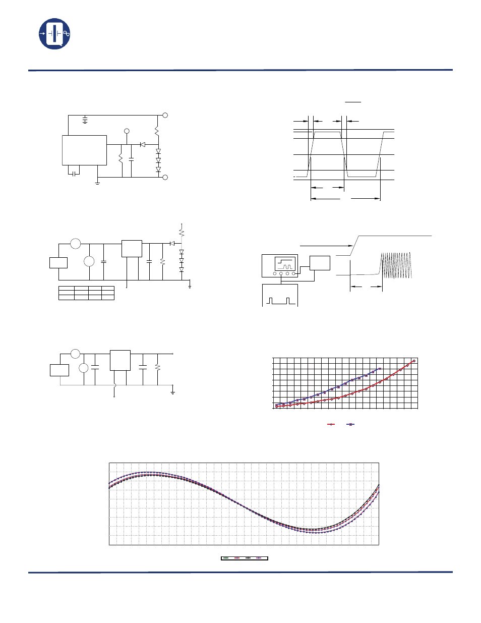
Frequency vs. Temperature Curve
-50
-40
-30
-20
-10
10
20
30
40
0
-55
-50
-45
-40
-35
-30
-25
-20
-15
-10
-5
0
5
10
15
20
25
30
35
40
45
50
55
60
65
70
75
80
85
90
95
100 105 110 115 120 125
SN2
SN3
SN4
SN1
Frequency Stability (PPM)
FREQUENCY STABILITY VERSUS TEMPERATURE QT1L -36MHz
Temperature (°C)
Vdd
GND
0.1xVdd
0.9xVdd
VOH
VOL
Tr
Tf
TH
T
0.5xVdd
SYMMETRY = x 100%
TH
T
Ts
Start-up box
Oscilloscope
DUT
Variable Ramp
54616B Agilent
TYPICAL SET-UP FOR START-UP TIME
Output Waveform (Typical)
Startup Time
Supply Current
Test Circuit
-
-
Output
Ground
0.1µF
15pF
Tristate Function
Power
supply
10k
mA
Vdc
+
+
+
(*)
or
0.01µF
(*) CL includes probe and jig capacitance
Typical test circuit for CMOS logic
Vdd
Out
GND
E/D
0
5
10
15
20
25
30
35
40
45
0.5
2
8
16 24 27 32 36
40 48 50 55 65
70 75 85 100 125 133 150 160
Freq(MHz)
Icc (mA)
TYPICAL SUPPLY CURRENT ICC (mA) AT 3.3Vdc & 5.0Vdc CMOS Logic NO LOAD
Icc 3.3V
Icc 5V
POWER
SUPPLY
+
-
mA
0.1µF
Vdc
-
Vdd OUT
OUT
GND
Typical test circuit for TTL logic.
0.01µF
Rs
(*) CL inclides the loading effect of the oscilloscope probe.
E/D
CL
+
+
-
RL
LOAD
6 TTL
10 TTL
CL(*)
12pF
20pF
RL
430Ω
270Ω
RS
10kΩ
6kΩ
or
Vdd
The Tristate function on pin 1 has a built-in pull-up resistor typical 50kΩ, so it can
be left floating or tied to Vdd without deteriorating the electrical performance.