Tvs diode arrays, Lightning surge protection- srda3.3 series, Diodes) – Littelfuse SRDA3.3 Series User Manual
Page 2: Sp4040
©2013 Littelfuse, Inc.
Specifi cations are subject to change without notice.
Please refer to
http://www.littelfuse.com
for current information.
2
TVS Diode Arrays
(SPA
®
Diodes)
Revision: June 14, 2013
Lightning Surge Protection- SRDA3.3 Series
SRDA3.3 Series
SP4040
Absolute Maximum Ratings
Electrical Characteristics (T
OP
= 25°C)
Thermal Information
Parameter
Rating
Units
SOIC Package
170
°C/W
Operating Temperature Range
-40 to 125
°C
Storage Temperature Range
-55 to 150
°C
Maximum Junction Temperature
150
°C
Maximum Lead Temperature (Soldering
20-40s) (SOIC - Lead Tips Only)
260
°C
CAUTION: Stresses above those listed in “Absolute Maximum Ratings” may cause
permanent damage to the device. This is a stress only rating and operation of the device
at these or any other conditions above those indicated in the operational sections of this
specifi cation is not implied.
1
Parameter is guaranteed by design and/or device characterization.
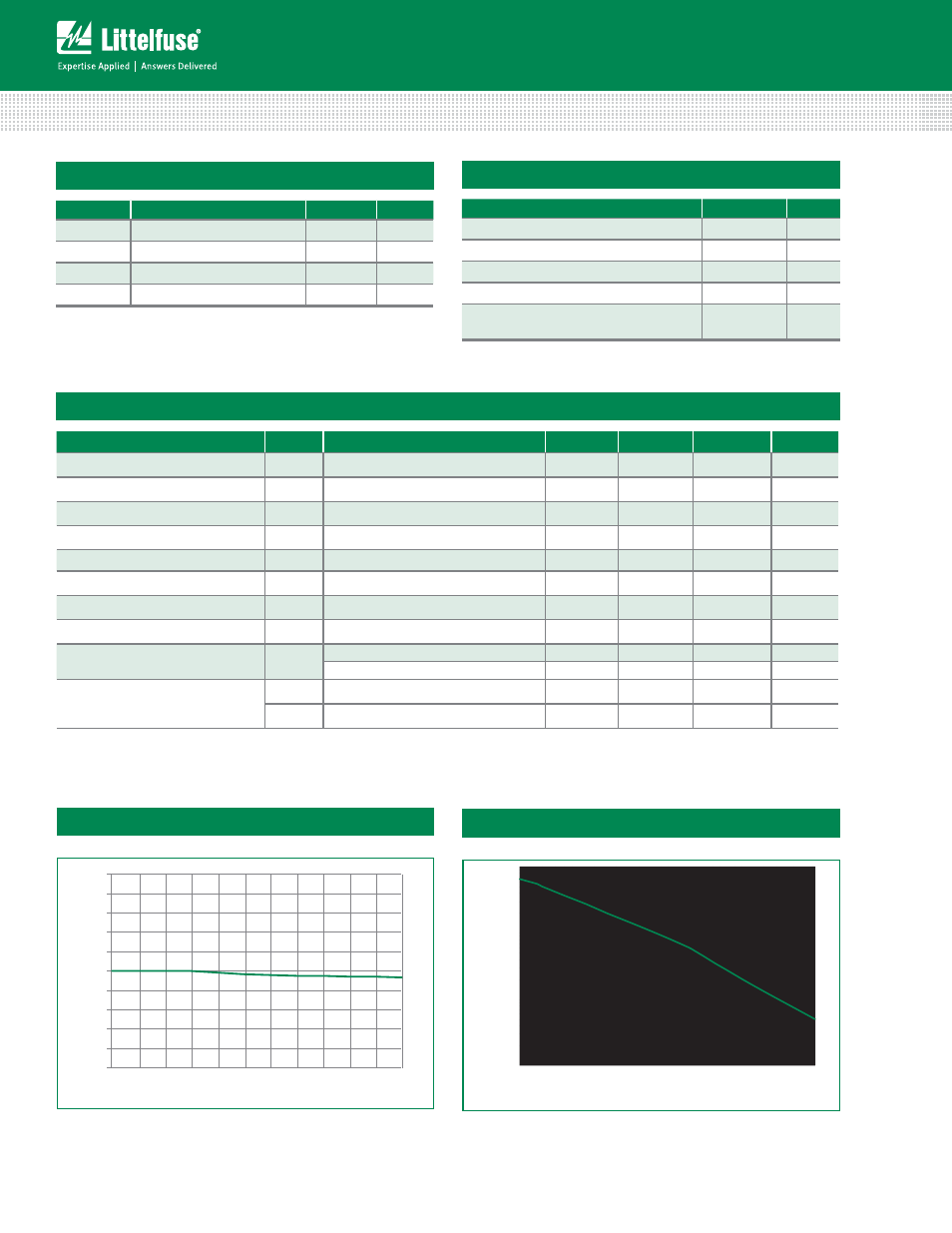
Normalized Capacitance vs. Bias Voltage
Symbol
Parameter
Value
Units
P
pk
Peak Pulse Power (8/20μs)
600
W
I
pp
Peak Pulse Current (8/20μs)
35
A
T
op
Operating Temperature
-40 to 125
°C
T
STOR
Storage Temperature
-55 to 150
°C
Parameter
Symbol
Test Conditions
Min
Typ
Max
Units
Reverse Stand-Off Voltage
V
RWM
I
T
≤1μA
-
-
3.3
V
Reverse Breakdown Voltage
V
BR
I
T
=2uA
3.5
-
-
V
Snap Back Voltage
V
SB
I
T
=50mA
2.9
-
-
V
Reverse Leakage Current
I
R
V
R
= 3.3V
-
-
1
μA
Clamping Voltage, Line-Ground
1
V
C
I
PP
= 1A, t
p
=8/20 μs
-
5.7
-
V
Clamping Voltage, Line-Ground
1
V
C
I
PP
= 10A, t
p
=8/20 μs
-
10.1
-
V
Clamping Voltage, Line-Ground
1
V
C
I
PP
= 30A, t
p
=8/20 μs
-
17.7
-
V
Dynamic Resistance, Line-Ground
1
R
DYN
( V
C2
-V
C1
)/(I
PP2
-I
PP1
)
-
0.5
-
Ω
ESD Withstand Voltage
1
V
ESD
IEC61000-4-2 (Contact Discharge)
±30
-
-
kV
IEC61000-4-2 (Air Discharge)
±30
-
-
kV
Diode Capacitance
1
C
I/O-I/O
Reverse
Bias=0V
-
4.0
-
pF
C
I/O-GND
Reverse
Bias=0V
-
8.0
-
pF
0.01
0.1
1
10
0.1
1
10
100
1000
Pulse Duration-tp(μS)
Peak Pulse
Po
wer
-P
pk
(kW)
Non-Repetitive Peak Pulse Power vs. Pulse Time
Bias Voltage (V)
Normalized Capacitance (pF)
0.0
0.2
0.4
0.6
0.8
1.0
1.2
1.4
1.6
1.8
2.0
0.0 0.3 0.6 0.9 1.2 1.5 1.8 2.1 2.4 2.7 3.0 3.3