Tvs diode arrays, Lightning surge protection- srda05 series, Diodes) – Littelfuse SRDA05 Series User Manual
Page 2: Sp4040, Absolute maximum ratings, Electrical characteristics (t, 25°c) thermal information, Non-repetitive peak pulse power vs. pulse time, Normalized capacitance vs. bias voltage
© 2013 Littelfuse, Inc.
Specifications are subject to change without notice.
Revised: 04/24/13
TVS Diode Arrays
(SPA
®
Diodes)
Lightning Surge Protection- SRDA05 Series
SP4040
Absolute Maximum Ratings
Symbol
Parameter
Value
Units
P
pk
Peak Pulse Power (8/20µs)
600
W
I
pp
Peak Pulse Current (8/20µs)
30
A
T
op
Operating Temperature
–40 to 125
°C
T
STOR
Storage Temperature
–55 to 150
°C
Electrical Characteristics (T
OP
= 25°C)
Thermal Information
Parameter
Rating
Units
SOIC Package
170
°C/W
Operating Temperature Range
–40 to 125
°C
Storage Temperature Range
–55 to 150
°C
Maximum Junction Temperature
150
°C
Maximum Lead Temperature (Soldering
20-40s) (SOIC - Lead Tips Only)
260
°C
Parameter
Symbol
Test Conditions
Min
Typ
Max
Units
Reverse Stand-Off Voltage
V
RWM
I
T
≤1µA
-
-
5.0
V
Reverse Leakage Current
I
R
V
R
= 5V
-
-
10
µA
Reverse Breakdown Voltage
V
BR
I
t
= 1mA
6
-
-
V
Clamping Voltage, Line-Ground
1
V
C
I
PP
= 1A, t
p
=8/20 µs
-
9.2
-
V
Clamping Voltage, Line-Ground
1
V
C
I
PP
= 2A, t
p
=8/20 µs
-
10.0
-
V
Clamping Voltage, Line-Ground
1
V
C
I
PP
= 10A, t
p
=8/20 µs
-
14.5
-
V
Clamping Voltage, Line-Ground
1
V
C
I
PP
= 25A, t
p
=8/20 µs
-
21.0
-
V
Dynamic Resistance, Line-Ground
1
R
DYN
( V
C2
-V
C1
)/(I
PP2
-I
PP1
)
-
0.8
-
W
ESD Withstand Voltage
1
V
ESD
IEC61000-4-2 (Contact Discharge)
±30
-
-
kV
IEC61000-4-2 (Air Discharge)
±30
kV
Diode Capacitance
1
C
I/O-I/O
Reverse Bias=0V
-
4.0
-
pF
C
I/O-GND
Reverse Bias=0V
-
8.0
-
pF
CAUTION: Stresses above those listed in “Absolute Maximum Ratings” may cause
permanent damage to the device. This is a stress only rating and operation of the device
at these or any other conditions above those indicated in the operational sections of this
specification is not implied.
1
Parameter is guaranteed by design and/or device characterization.
0.01
0.1
1
10
0.1
1
10
100
1000
Pulse Duration-tp(µS)
Peak Pulse
Po
we
r-
P
pk
(kW)
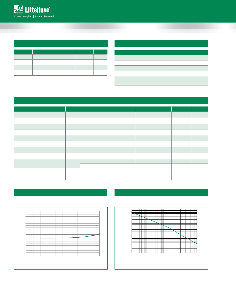
Non-Repetitive Peak Pulse Power vs. Pulse Time
0.0
0.5
1.0
1.5
2.0
2.5
3.0
3.5
4.0
4.5
5.0
Bias Voltage (V)
Normalized Capacitance (pF) Cj(VR)/Cj(VR=0)
1.0
1.2
1.4
1.6
1.8
2.0
2.2
2.4
2.5
0.8
0.6
0.4
0.2
0.0
Normalized Capacitance vs. Bias Voltage