Clamping voltage vs. ipp, Pulse waveform, Soldering parameters – Littelfuse SP4021 Series User Manual
Page 3: Product characteristics, Tvs diode arrays, Lightning surge protection- sp4021 series, Diodes), Sp4021, Clamping voltage vs. i, Soldering parameters product characteristics
3
©2013 Littelfuse, Inc.
Specifications are subject to change without notice.
Please refer to
www.littelfuse.com
for current information.
TVS Diode Arrays
(SPA
®
Diodes)
Revision: July 12, 2013
Lightning Surge Protection- SP4021 Series
SP4021
SP4021 Series
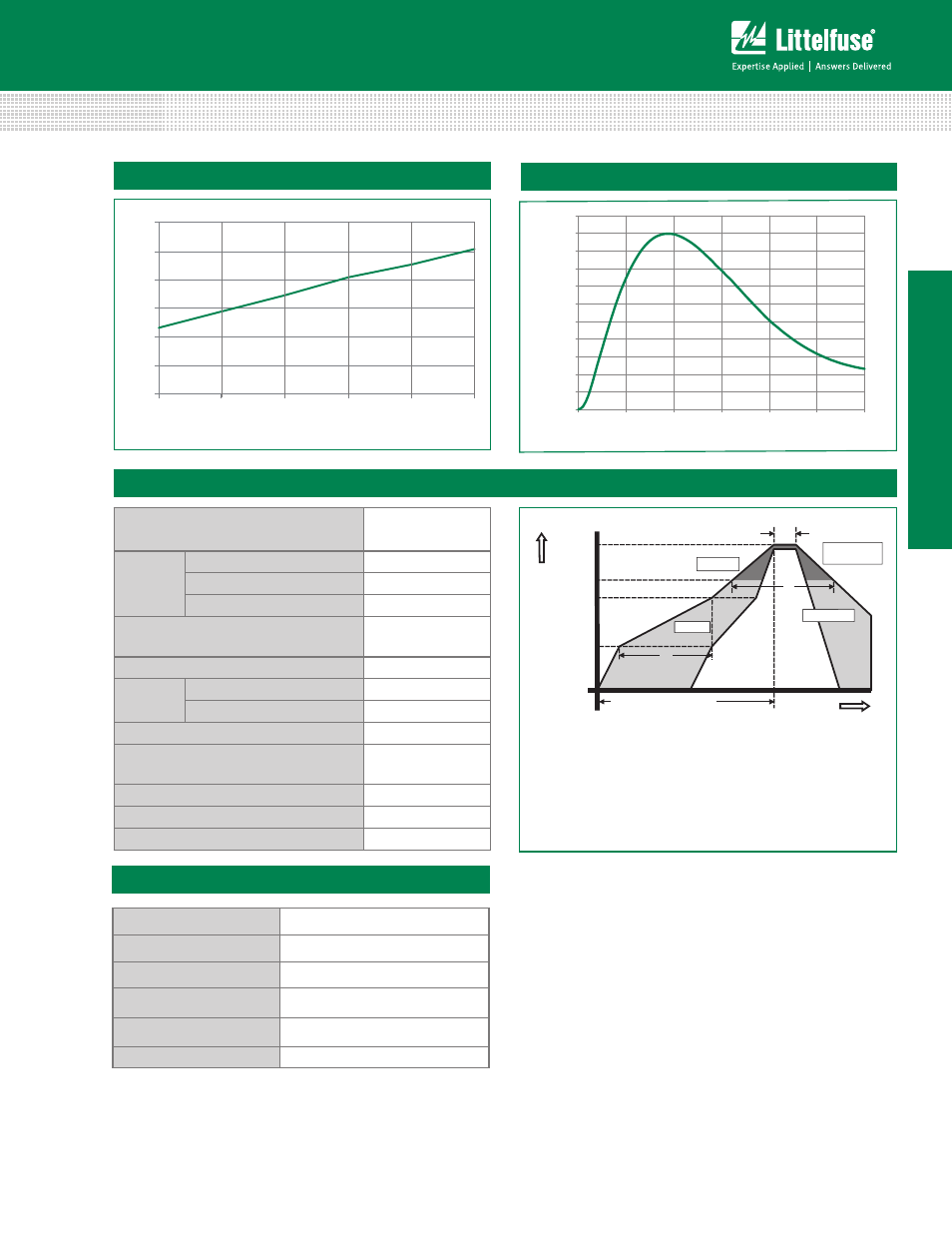
Clamping Voltage vs. I
PP
25.0
10.0
20.0
5.0
15.0
Cl
am
p
Vo
lt
age
(V
C
)
0.0
4.0
8.0
12.0
16.0
20.0
24.0
1.0
Peak Pulse Current-I
PP
(A)
Time
Temperature
T
P
T
L
T
S(max)
T
S(min)
25
t
P
t
L
t
S
time to peak temperature
Preheat
Preheat
Ramp-up
Ramp-up
Ramp-down
Ramp-do
Critical Zone
T
L
to T
P
Critical Zone
T
L
to T
P
Reflow Condition
Pb – Free assembly
Pre Heat
- Temperature Min (T
s(min)
)
150°C
- Temperature Max (T
s(max)
)
200°C
- Time (min to max) (t
s
)
60 – 180 secs
Average ramp up rate (Liquidus) Temp
(T
L
) to peak
3°C/second max
T
S(max)
to T
L
- Ramp-up Rate
3°C/second max
Reflow
- Temperature (T
L
) (Liquidus)
217°C
- Temperature (t
L
)
60 – 150 seconds
Peak Temperature (T
P
)
260
+0/-5
°C
Time within 5°C of actual peak
Temperature (t
p
)
20 – 40 seconds
Ramp-down Rate
6°C/second max
Time 25°C to peak Temperature (T
P
)
8 minutes Max.
Do not exceed
260°C
Soldering Parameters
Product Characteristics
Lead Plating
Matte Tin
Lead Material
Copper Alloy
Lead Coplanarity
0.0004 inches (0.102mm)
Substitute Material
Silicon
Body Material
Molded Epoxy
Flammability
UL 94 V-0
Notes :
1. All dimensions are in millimeters
2. Dimensions include solder plating.
3. Dimensions are exclusive of mold flash & metal burr.
4. Blo is facing up for mold and facing down for trim/form, i.e. reverse trim/form.
5. Package surface matte finish VDI 11-13.
Pulse Waveform
0%
10%
20%
30%
40%
50%
60%
70%
80%
90%
100%
110%
0.0 5.0 10.0 15.0 20.0 25.0 30.0
Time (μs)
Percent of
I
PP