Gas discharge tube (gdt) products, Pmt3(310) series, Recommended process parameters – Littelfuse PMT3(310) Series User Manual
Page 2: Product characteristics
©2011 Littelfuse, Inc.
Gas Discharge Tube (GDT) Products
Revised: June 27, 2011
Specifications are subject to change without notice.
Please refer to www.littelfuse.com for current information.
Customer should verify actual device performance in their specific applications.
PMT3(310) Series
PMT3(310) Series
Product Characteristics
Materials
%VMM5JO1MBUF.JDSPOT
XJUI$FSBNJD*OTVMBUPS
Product Marking
-JUUFMGVTFA-'NBSLJOH
7PMUBHFBOE
date code.
Glow to arc
transition current
_"NQ
Glow Voltage
_7PMUT
Reflow Condition
Pb – Free assembly
Pre Heat
- Temperature Min (T
s(min)
)
¡$
- Temperature Max (T
s(max)
)
¡$
- Time (Min to Max) (t
s
)
oTFDT
Average ramp up rate (Liquidus Temp
(T
L
) to peak
¡$TFDPOENBY
T
S(max)
to T
L
- Ramp-up Rate
¡$TFDPOENBY
Reflow
- Temperature (T
L
) (Liquidus)
¡$
- Temperature (t
L
)
oTFDPOET
Peak Temperature (T
P
)
¡$
Time within 5°C of actual peak
Temperature (t
p
)
10 – 30 seconds
Ramp-down Rate
¡$TFDPOENBY
Time 25°C to peak Temperature (T
P
)
NJOVUFT.BY
Do not exceed
¡$
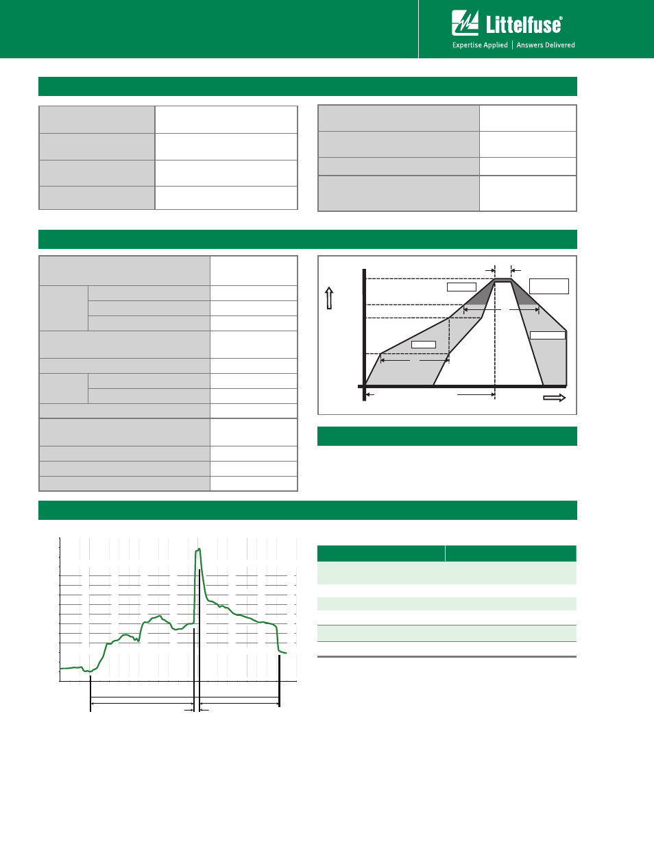
Soldering Parameters - Reflow Soldering (Surface Mount Devices)
Time
T
emperature
T
P
T
L
T
S(max)
T
S(min)
25
t
P
t
L
t
S
time to peak temperature
(t 25ºC to peak)
Ramp-down
Ramp-up
Preheat
Critical Zone
T
L
to T
P
Soldering Parameters - Wave Soldering (Thru-Hole Devices)
Soldering Parameters - Hand Soldering
Dwell Time
0
20
40
60
80
100
120
140
160
180
200
220
240
260
280
300
0
10
20
30
40
50
60
70
80
90
100
110
120
130
140
150
160
170
180
190
200
210
220
230
240
Time (Seconds)
T
emperature (°C) - Measured on
bottom side
of
board
Cooling Time
Preheat Time
Wave Parameter
Lead-Free Recommendation
Preheat:
%FQFOETPO'MVY"DUJWBUJPO5FNQFSBUVSF
5ZQJDBM*OEVTUSZ3FDPNNFOEBUJPO
5FNQFSBUVSF.JOJNVN
100
¡
$
5FNQFSBUVSF.BYJNVN
¡
$
1SFIFBU5JNF
TFDPOET
Solder Pot Temperature:
¡
$.BYJNVN
Solder Dwell Time:
TFDPOET
Recommended Process Parameters:
4PMEFS*SPO5FNQFSBUVSF¡$¡$
)FBUJOH5JNFTFDPOETNBY
/PUF4VSHF"SSFTUPSTXJUIB'BJMTBGFmechanism should be
individually
FYBNJOFE after soldering
Storage and Operational
Temperature
UP¡$
Transverse Voltage (Delay Time)
5FTUFEUP*5653FD,
4FD
Arc Voltage
_UP7PMUT
Holdover Voltage
5FTUFEUP*5653FD,3&"1&
N4