Varistor products, High reliability varistors, Radiation hardness – Littelfuse High Reliability Varistors User Manual
Page 6

© 2013 Littelfuse, Inc.
206
Revised: May 8, 2013
Varistor Products
High Reliability Varistors
High Reliability Varistors
Specifications are subject to change without notice.
Please refer to www.littelfuse.com/series/za hirel.html or /db hirel.html
for current information.
Counterclockwise rotation of the V-I characteristics is
observed in Silicon devices at high neutron irradiation
levels; in other words, increasing leakage at low current
levels and increasing clamping voltage at higher current
levels.
The solid and open circles for a given fluence represent the
high and low breakdown currents for the sample of devices
tested. Note that there is a marked decrease in current (or
energy) handling capability with increased neutron fluence.
Failure threshold of Silicon semiconductor junctions is
further reduced when high or rapidly increasing currents
are applied. Junctions develop hot spots, which enlarge
until a short occurs if current is not limited or quickly
removed.
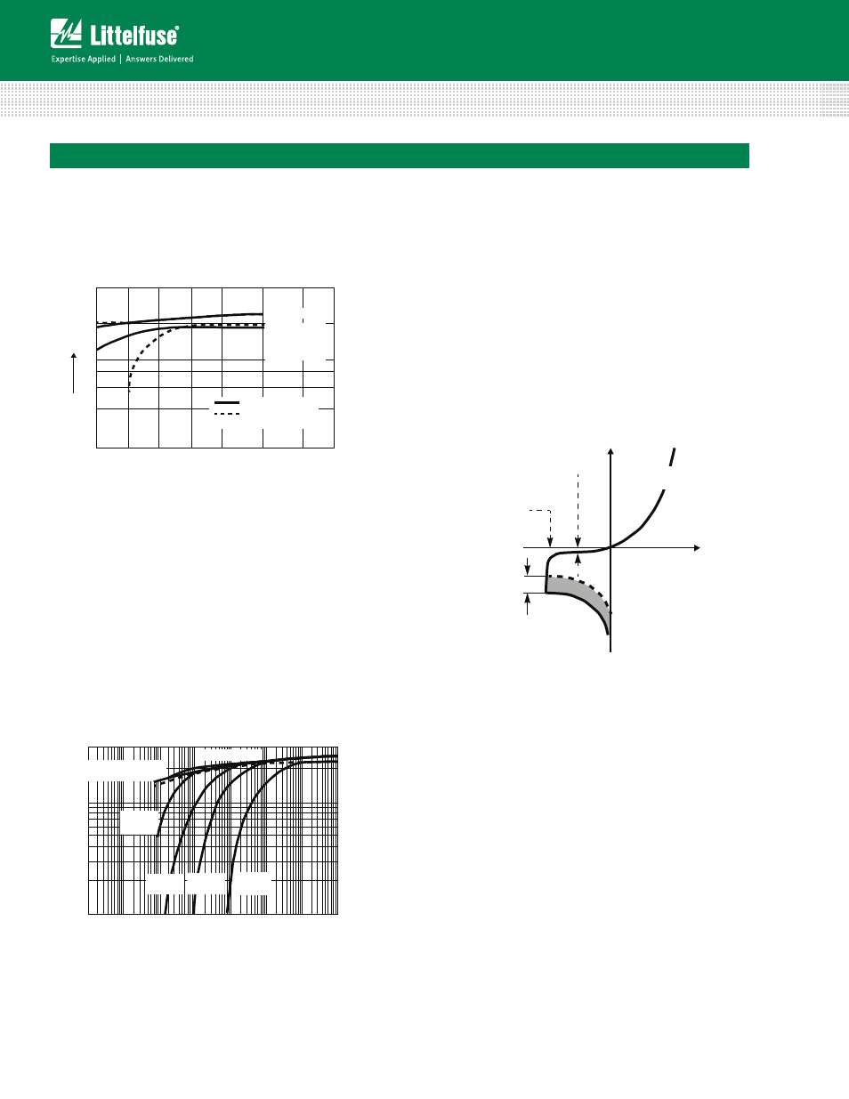
The characteristic voltage current relationship of a P– N
Junction is shown below.
At low reverse voltage, the device will conduct very little
current (the saturation current). At higher reverse voltage
VBO (breakdown voltage),the current increases rapidly as
the electrons are either pulled by the electric field (Zener
effect) or knocked out by other electrons (avalanching). A
further increase in voltage causes the device to exhibit a
negative resistance characteristic leading to secondary
breakdown.
This manifests itself through the formation of hotspots,
and irreversible damage occurs. This failure threshold
decreases under neutron irradiation for Zeners, but not for
Z
N
O Varistors.
Gamma Radiation
Radiation damage studies were performed on type
V130LA2 varistors. Emission spectra and V-I characteristics
were collected before and after irradiation with 106 rads
Co60 gamma radiation. Both show no change, within
experimental error, after irradiation.
For space applications, an extremely important property of a
protection device is its response to imposed radiation effects.
Electron Irradiation
A Littelfuse MOV and a Silicon transient suppression diode
were exposed to electron irradiation. The V-I curves, before
and after test, are shown below.
It is
apparent that the Littelfuse MOV was virtually unaffected,
even at the extremely high dose of 108 rads, while the
Silicon transient suppression diode showed a dramatic
increase in leakage current.
Neutron Effects
A second MOV-Zener comparison was made in response to
neutron fluence. The selected devices were equal in area.
Figure 2 shows the clamping voltage response of the MOV
and the Zener to neutron irradiation to as high as 1015 N/
cm
2
. It is apparent that in contrast to the large change in
the Zener, the MOV is unaltered. At highercurrents where
the MOV’s clamping voltage is again unchanged, the Zener
device clamping voltage increases by as much as 36%.
V
200
100
80
60
40
20
10
8
10
6
10
4
10
2
SILICON
TRANSIENT
CURRENT (A)
PRE TEST
10
8
RADS,
18MeV ELECTRONS
LITTELFUSE MOV
SUPPRESSION
DIODE
FIGURE 1. RADIATION SENSITIVITY OF LITTELFUSE V130LA1
AND SILICON TRANSIENT SUPPRESSION DIODE
Radiation Hardness
VO
LT
S
200
100
80
60
40
20
10
8
10
10
7
10
6
10
4
10
3
AMPERES
300
50
30
10
10
10
5
1.5K 200
AT 10
15
1.5K 200 INITIAL
VARISTOR V130A2
INITIAL AT 10
15
1.5K 200
AT 10
14
1.5K 200
AT 10
13
1.5K 200
AT 10
12
FIGURE 2. V-I CHARACTERISTIC RESPONSE TO NEUTRON
IRRADIATION FOR MOV AND ZENER DIODE
DEVICES
SATURATION
CURRENT
BREAKDOWN
VOLTAGE
I
V
REDUCTION IN
FAILURE STRESSHOLD
BY RADIAL
SECONDARY
BREAKDOWN
REVERSE
BIAS
FORWARD
BIAS
FIGURE 3. V-I CHARACTERISTIC OF PN-JUNCTION
