Tvs diode arrays, Lightning surge protection - sp4060 series, Diodes) – Littelfuse SP4060 Series User Manual
Page 3: Soldering parameters package dimensions — msop10, Solder pad layout
© 2013 Littelfuse, Inc.
Specifications are subject to change without notice.
Revised: 04/24/13
TVS Diode Arrays
(SPA
®
Diodes)
Lightning Surge Protection - SP4060 Series
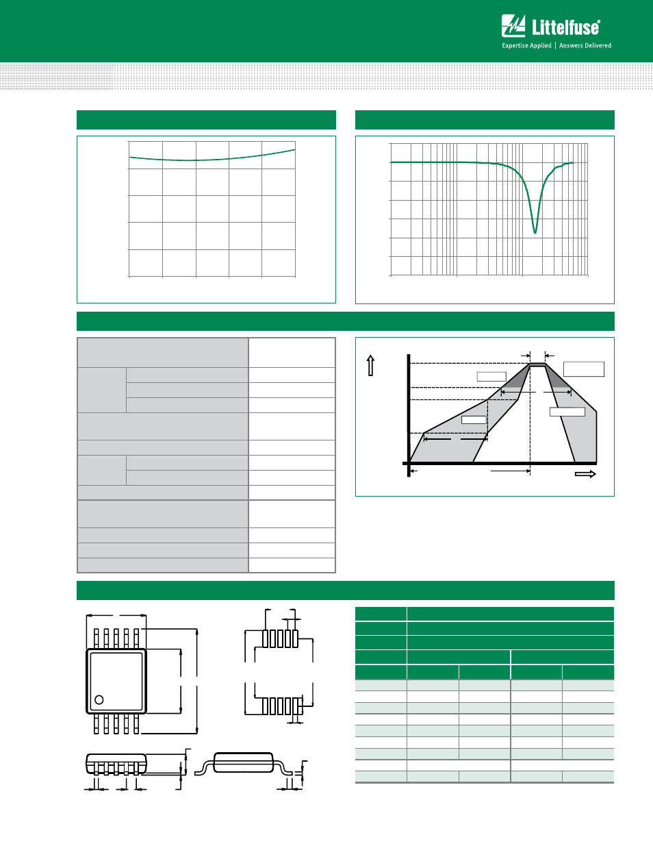
Capacitance vs. Bias
Insertion Loss (S21) I/O to GND
0.0
1.0
2.0
3.0
4.0
5.0
0.0 0.5 1.0 1.5 2.0 2.5
DC Bias (V)
Capacitance (pF)
-30
-25
-20
-15
-10
-5
0
5
0
0
0
0
1
0
0
0
1
0
0
1
0
1
Frequency (MHz)
Attenuation (dB)
Time
Te
mperatur
e
T
P
T
L
T
S(max)
T
S(min)
25
t
P
t
L
t
S
time to peak temperature
Preheat
Preheat
Ramp-up
Ramp-up
Ramp-down
Ramp-do
Critical Zone
T
L
to T
P
Critical Zone
T
L
to T
P
Reflow Condition
Pb – Free assembly
Pre Heat
- Temperature Min (T
s(min)
)
150°C
- Temperature Max (T
s(max)
)
200°C
- Time (min to max) (t
s
)
60 – 180 secs
Average ramp up rate (Liquidus) Temp
(T
L
) to peak
3°C/second max
T
S(max)
to T
L
- Ramp-up Rate
3°C/second max
Reflow
- Temperature (T
L
) (Liquidus)
217°C
- Temperature (t
L
)
60 – 150 seconds
Peak Temperature (T
P
)
260
+0/-5
°C
Time within 5°C of actual peak
Temperature (t
p
)
20 – 40 seconds
Ramp-down Rate
6°C/second max
Time 25°C to peak Temperature (T
P
)
8 minutes Max.
Do not exceed
260°C
Soldering Parameters
Package Dimensions — MSOP10
Package
MSOP
Pins
10
JEDEC
MO-187
Millimeters
Inches
DIM
Min
Max
Min
Max
A
-
1.10
-
0.043
A1
0.00
0.15
0.000
0.006
B
0.17
0.27
0.007
0.011
c
0.08
0.23
0.003
0.009
D
2.90
3.10
0.114
0.122
E
4.67
5.10
0.184
0.200
E1
2.90
3.10
0.114
0.122
e
0.50 BSC
0.020 BSC
L
0.40
0.80
0.016
0.032
B
e
A1
A
2
1
E1
E
10
D
L
C
0.32
[0.0126]
4.24
[0.1
669]
1.
04
[0.0409
]
5.28
[0.2079
]
3.20
[0.1
260]
0.50
[0.0197]
2.00
[0.0787]
Solder Pad Layout