Tvs diode arrays, General purpose esd protection - sp725 series, Diodes) – Littelfuse SP725 Series User Manual
Page 5
© 2013 Littelfuse, Inc.
Specifications are subject to change without notice.
Revised: 04/24/13
TVS Diode Arrays
(SPA
®
Diodes)
General Purpose ESD Protection - SP725 Series
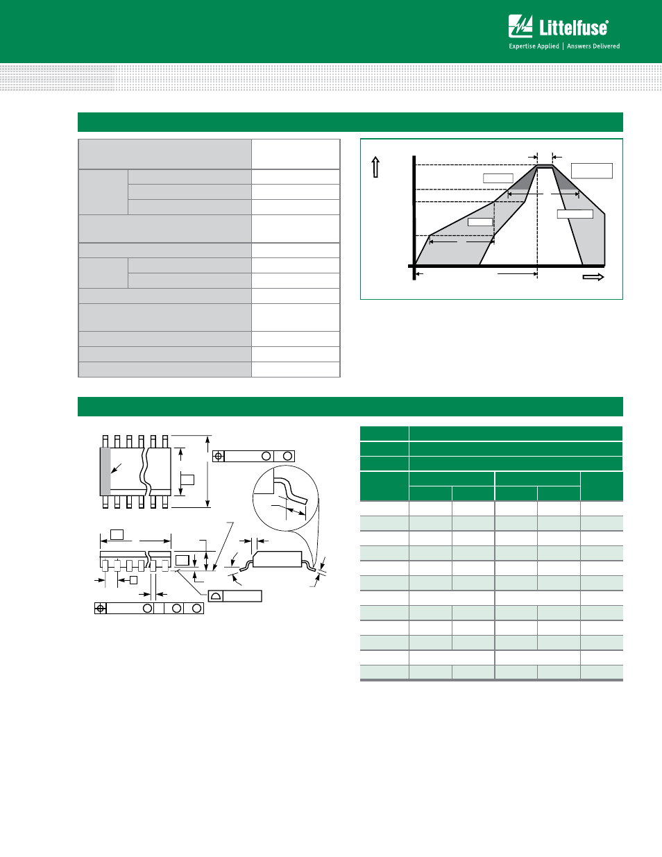
Package Dimensions — Small Outline Plastic Packages (SOIC)
Time
Te
mperatur
e
T
P
T
L
T
S(max)
T
S(min)
25
t
P
t
L
t
S
time to peak temperature
Preheat
Preheat
Ramp-up
Ramp-up
Ramp-down
Ramp-do
Critical Zone
T
L
to T
P
Critical Zone
T
L
to T
P
Reflow Condition
Pb – Free assembly
Pre Heat
- Temperature Min (T
s(min)
)
150°C
- Temperature Max (T
s(max)
)
200°C
- Time (min to max) (t
s
)
60 – 180 secs
Average ramp up rate (Liquidus) Temp
(T
L
) to peak
5°C/second max
T
S(max)
to T
L
- Ramp-up Rate
5°C/second max
Reflow
- Temperature (T
L
) (Liquidus)
217°C
- Temperature (t
L
)
60 – 150 seconds
Peak Temperature (T
P
)
260
+0/-5
°C
Time within 5°C of actual peak
Temperature (t
p
)
20 – 40 seconds
Ramp-down Rate
5°C/second max
Time 25°C to peak Temperature (T
P
)
8 minutes Max.
Do not exceed
260°C
Soldering Parameters
INDEX
AREA
E
D
N
1
2
3
-B-
0.25(0.010)
C A
M
B S
e
-A-
L
B
M
-C-
A1
A
SEATING PLANE
0.10(0.004)
h x 45
o
C
H
µ
0.25(0.010)
B
M
M
Notes:
1. Symbols are defined in the “MO Series Symbol List” in Section 2.2 of Publication
Number 95.
2. Dimensioning and tolerancing per ANSI Y14.5M-1982.
3. Dimension “D” does not include mold flash, protrusions or gate burrs. Mold flash,
protrusion and gate burrs shall not exceed 0.15mm (0.006 inch) per side.
4. Dimension “E” does not include interlead flash or protrusions. Interlead flash and
protrusions shall not exceed 0.25mm (0.010 inch) per side.
5. The chamfer on the body is optional. If it is not present, a visual index feature must be
located within the crosshatched area.
6. “L” is the length of terminal for soldering to a substrate.
7. “N” is the number of terminal positions.
8. Terminal numbers are shown for reference only.
9. The lead width “B”, as measured 0.36mm (0.014 inch) or greater above the seating
plane, shall not exceed a maximum value of 0.61mm (0.024 inch).
10. Controlling dimension: MILLIMETER. Converted inch dimensions are not necessarily
exact.
Package
SOIC
Pins
8
JEDEC
MS-012
Millimeters
Inches
Notes
Min
Max
Min
Max
A
1.35
1.75
0.0532
0.0688
-
A1
0.10
0.25
0.0040
0.0098
-
B
0.33
0.51
0.013
0.020
9
C
0.19
0.25
0.0075
0.0098
-
D
4.80
5.00
0.1890
0.1968
3
E
3.80
4.00
0.1497
0.1574
4
e
1.27 BSC
0.050 BSC
-
H
5.80
6.20
0.2284
0.2440
-
h
0.25
0.50
0.0099
0.0196
5
L
0.40
1.27
0.016
0.050
6
N
8
8
7
µ
0
o
8
o
0
o
8
o
-